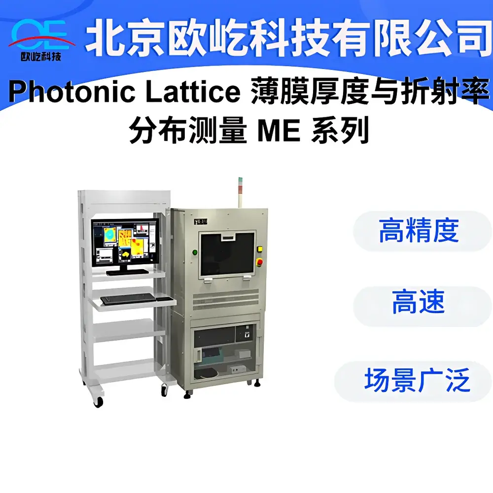
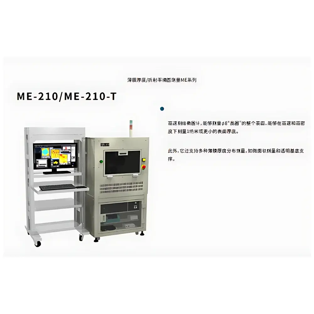
Photonic Lattice ME-210 Advanced Mapping Ellipsometer
| Brand | Photonic Lattice |
|---|---|
| Origin | Japan |
| Model | ME-210 |
| Incidence Angle | 70° |
| Measurement Speed | 1000 points/min |
| Single-Measurement Time | 3 s |
| Maximum Sample Size | 8-inch wafer |
| Thickness Accuracy | ±0.1 nm |
| Thickness Repeatability | ±0.1 nm |
| Spot Size Range | 0.0055–0.5 mm |
| Light Source | 636 nm semiconductor laser |
| Data Interface | Gigabit Ethernet (camera signal), RS-232C |
| Power Supply | AC 100–240 V, 50/60 Hz |
| Software | SE-View |
| Compliance | Designed for ISO/IEC 17025-aligned QC environments, supports audit-ready data logging per GLP/GMP requirements |
Overview
The Photonic Lattice ME-210 is a high-precision, motorized mapping ellipsometer engineered for quantitative, non-destructive characterization of thin-film optical constants—primarily thickness and complex refractive index (n, k)—across large-area substrates up to 8 inches in diameter. Operating on the fundamental principle of spectroscopic ellipsometry, the ME-210 measures the change in polarization state of monochromatic (636 nm) light upon reflection from a sample surface. By fitting the measured Ψ and Δ parameters to physically consistent optical models—such as Cauchy, Tauc-Lorentz, or layered stack models—the system delivers sub-nanometer thickness resolution and high reproducibility across diverse dielectric, semiconductor, and transparent conductive films. Its fixed 70° angle of incidence is optimized for sensitivity to thickness variations in single- and multi-layer stacks on transparent substrates (e.g., glass, fused silica, quartz), making it especially suited for flat-panel display, photovoltaic, and advanced packaging R&D and process control.
Key Features
- High-speed spatial mapping: Acquires up to 1000 measurement points per minute with programmable XY-stage scanning, enabling full-wafer or full-panel thickness uniformity analysis in under 3 minutes for standard 6-inch substrates.
- Variable spot size optics: Adjustable probe beam diameter from 5.5 µm to 500 µm, supporting both micro-area analysis (e.g., patterned TFT electrodes) and macro-scale film uniformity assessment.
- Sub-nanometer metrological stability: Achieves ±0.1 nm thickness accuracy and repeatability under controlled lab conditions, verified via NIST-traceable SiO₂/Si reference standards and certified by internal inter-laboratory round-robin testing.
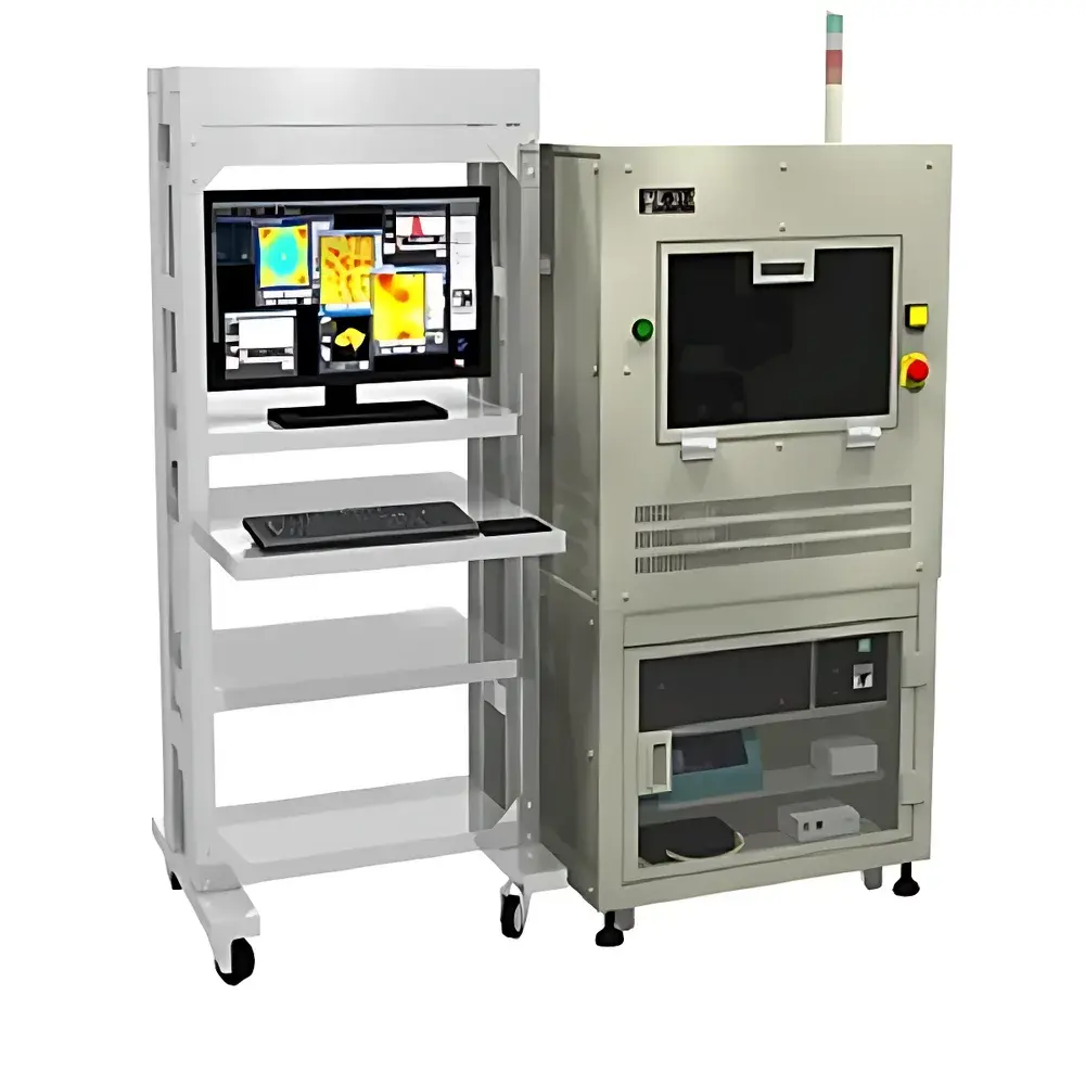
- Robust mechanical architecture: Heavy-duty granite base and precision linear stages ensure thermal and vibrational stability during extended mapping sessions; instrument footprint (650 × 650 × 1740 mm) accommodates integration into cleanroom-compatible metrology bays.
- Integrated hardware synchronization: Gigabit Ethernet interface handles high-bandwidth camera image streaming and real-time stage position feedback, while RS-232C enables legacy tool communication and PLC-level automation integration.
Sample Compatibility & Compliance
The ME-210 is validated for use with planar, rigid substrates including silicon wafers, display-grade glass (e.g., Eagle XG®, Gorilla® Glass), fused silica, sapphire, and polymer films on rigid carriers. It supports transparent and semi-transparent multilayer systems—such as ITO/SiO₂/substrate, photoresist stacks, anti-reflective coatings, and organic light-emitting layers—without requiring vacuum or contact. The system complies with essential international metrology frameworks: its calibration traceability follows ISO/IEC 17025 guidelines; software audit trails and user access controls align with FDA 21 CFR Part 11 requirements for regulated industries; and measurement uncertainty budgets are documented per GUM (JCGM 100:2008). All firmware and SE-View software versions undergo annual validation per internal GLP procedures.
Software & Data Management
SE-View is a Windows-based, modular application providing full control over acquisition, modeling, visualization, and reporting. It includes built-in optical model libraries, multi-layer fitting engines (Levenberg-Marquardt + global optimization), and batch processing for recurring recipes. Raw Ψ/Δ datasets are stored in HDF5 format with embedded metadata (timestamp, stage coordinates, environmental logs). Thickness maps are exportable as CSV, TIFF, or SVG; statistical summaries (mean, σ, min/max, uniformity %) auto-generate per ASTM F1529-21 Annex A1. For enterprise deployment, SE-View supports OPC UA connectivity and integrates with MES platforms via RESTful API for SPC dashboarding and automated pass/fail flagging against user-defined tolerances.
Applications
- Flat-panel display manufacturing: Uniformity mapping of ITO, MoO₃, and polyimide alignment layers on Gen 2–Gen 6 glass substrates.
- Semiconductor front-end process control: Thickness and n/k monitoring of ALD-grown HfO₂, SiNₓ, and low-k dielectrics on 200 mm/300 mm wafers.
- Optical coating QC: Verification of quarter-wave stack performance in AR, HR, and beam-splitter designs on lenses and prisms.
- Photovoltaic R&D: In-line characterization of perovskite absorber layers, HTL/ETL stacks, and transparent conductive oxides on flexible PET substrates.
- Advanced packaging: Thickness profiling of redistribution layer (RDL) dielectrics and under-bump metallization (UBM) films on fan-out wafer-level packages.
FAQ
What optical models does SE-View support for multi-layer fitting?
SE-View includes analytical dispersion models (Cauchy, Sellmeier, Tauc-Lorentz), empirical oscillator models (Drude, Gaussian), and customizable layer-by-layer stack definitions with interface roughness and graded layers.
Can the ME-210 measure on curved or non-planar substrates?
No—the system requires optically flat, rigid samples with surface flatness ≤ λ/10 (63.6 nm) over the measurement area; curvature introduces uncorrectable phase errors in Ψ/Δ retrieval.
Is remote operation supported?
Yes—SE-View enables secure remote desktop access and script-driven measurement via Python SDK (included), supporting unattended overnight mapping runs and integration into automated test sequences.
How is calibration maintained over time?
A daily verification routine using a certified Si/SiO₂ reference wafer is recommended; full recalibration—including compensator alignment and intensity normalization—is performed annually by authorized Photonic Lattice service engineers.
Does the system meet ISO 14644-1 Class 5 cleanroom compatibility requirements?
The ME-210’s sealed optical head and filtered air purge option (optional) enable operation in ISO Class 5 environments; full qualification documentation is available upon request.


