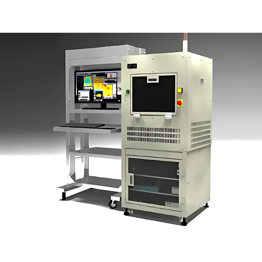
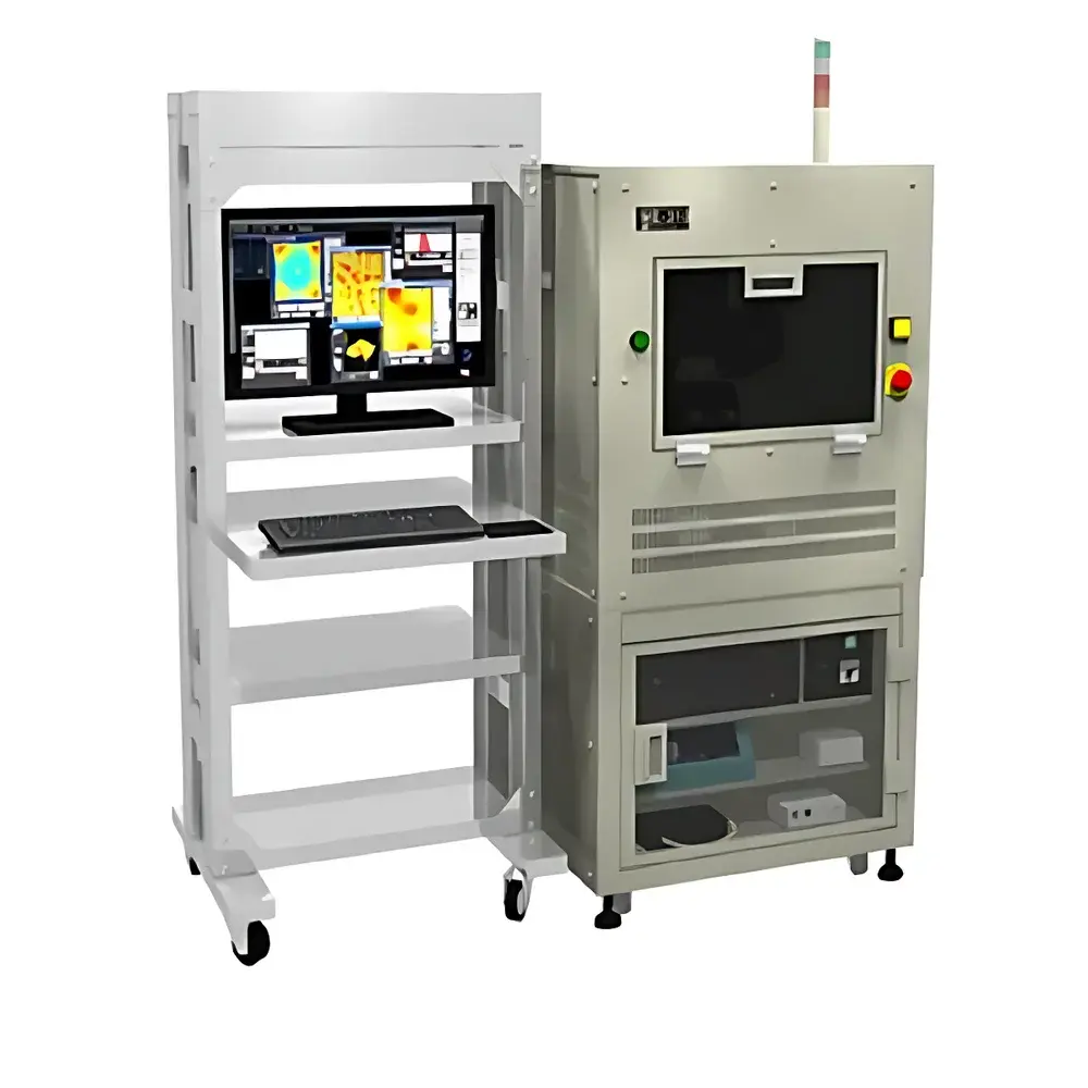
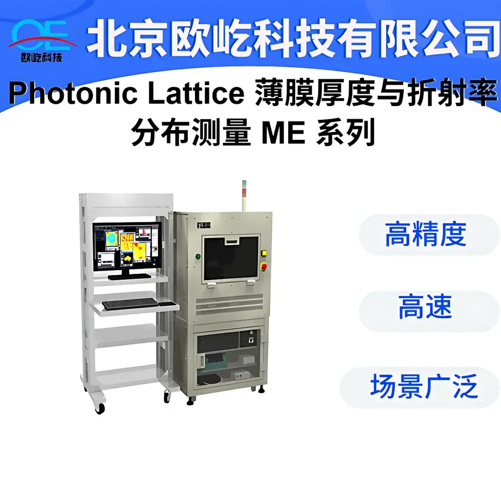
Photonic Lattice ME-210 / ME-210-T Compact Desktop Ellipsometer
| Brand | Photonic Lattice |
|---|---|
| Origin | Japan |
| Model | ME-210 / ME-210-T |
| Incident Angle | 70° |
| Measurement Speed | 1,000 points/min |
| Single-Measurement Time | 3 s |
| Maximum Sample Size | 8-inch (200 mm) diameter |
| Thickness Accuracy | ±0.1 nm |
| Thickness Repeatability | ±0.1 nm |
Overview
The Photonic Lattice ME-210 and ME-210-T are compact, high-precision desktop ellipsometers engineered for rapid, non-contact characterization of thin-film optical constants and thickness profiles on planar substrates. Based on the fundamental principles of spectroscopic ellipsometry—measuring the change in polarization state of reflected light—the system quantifies the complex dielectric function (n + ik) and film thickness with sub-nanometer resolution. These instruments operate at a fixed wavelength of 636 nm (semiconductor laser source) and a precisely controlled incident angle of 70°, optimizing sensitivity for transparent and semi-transparent dielectric films—including ITO, SiO₂, SiNₓ, photoresists, polymer alignment layers, and anti-reflective coatings—on glass, silicon, quartz, and crystalline substrates. Designed for integration into R&D labs and inline QC environments, the ME-210 series delivers metrology-grade performance without requiring vacuum chambers or complex optical alignment.
Key Features
- Sub-nanometer thickness accuracy and repeatability (±0.1 nm) across homogeneous and laterally graded films
- High-speed mapping capability: up to 1,000 measurement points per minute, enabling full-wafer or large-area substrate profiling within minutes
- Compact footprint (250 × 175 × 218.3 mm; 4 kg) with integrated laser source, detector, and motorized stage—no external optics table required
- Dual configuration options: ME-210 (manual XY stage) and ME-210-T (motorized translation stage with programmable positioning for automated grid scans)
- Fixed-angle, single-wavelength architecture ensures long-term stability and eliminates calibration drift associated with goniometric mechanisms
- Robust mechanical design compliant with ISO 14644-1 Class 8 cleanroom compatibility for semiconductor and display manufacturing support
Sample Compatibility & Compliance
The ME-210/ME-210-T supports flat, rigid substrates up to 200 mm (8-inch) in diameter and ≤10 mm in thickness. Compatible materials include fused silica, borosilicate glass (e.g., Eagle XG®, AF32®), silicon wafers (polished or oxidized), sapphire, CaF₂, and flexible polymer films mounted on carriers. The system is routinely deployed in applications governed by ASTM E1935 (Standard Test Method for Determining Optical Constants of Thin Films), ISO 15027-1 (Optics and photonics — Spectroscopic ellipsometry — Part 1: General principles), and JIS K 7105 (Testing methods for optical properties of plastics). Its measurement traceability aligns with NIST-traceable reference standards for refractive index and thickness, supporting GLP-compliant documentation workflows.
Software & Data Management
Controlled via SE-View™ software (Windows 10/11 x64), the platform provides real-time data acquisition, multi-layer optical modeling (Cauchy, Tauc-Lorentz, B-Spline parameterization), and spatial mapping visualization. All raw Ψ/Δ values, fitted parameters, and confidence intervals are stored in HDF5 format with embedded metadata (timestamp, operator ID, instrument serial number, environmental conditions). Audit trails comply with FDA 21 CFR Part 11 requirements when configured with user authentication, electronic signatures, and immutable log archiving. Data export supports CSV, ASCII, and industry-standard .mat formats for integration with MATLAB®, Python-based analysis pipelines, and MES/QMS platforms.
Applications
- Thickness uniformity mapping of transparent conductive oxides (TCOs) on display glass substrates
- Process validation of spin-coated photoresist and organic semiconductor layers in OLED and microLED fabrication
- Quantification of residual stress-induced birefringence in tempered glass and polymer lenses via phase difference imaging
- In-line monitoring of anti-reflective and hard-coating deposition on optical components
- Characterization of liquid crystal alignment layers (e.g., polyimide) for pretilt angle and surface anisotropy assessment
- Research-grade analysis of 2D material monolayers (MoS₂, WS₂) and van der Waals heterostructures on Si/SiO₂
FAQ
What is the minimum measurable film thickness?
The system reliably resolves films as thin as 0.3 nm (e.g., native oxide on Si) under optimal signal-to-noise conditions. Sub-angstrom sensitivity is achievable for high-contrast interfaces using averaging protocols.
Can the ME-210-T perform automated multi-point measurements across non-standard substrates?
Yes—SE-View™ supports custom coordinate import (CSV), irregular boundary definition, and adaptive step sizing for non-circular or clipped wafers, masks, or display panels.
Is temperature-controlled sample stage available as an option?
An optional Peltier-cooled stage (−10 °C to +80 °C, ±0.1 °C stability) is available for thermal expansion and phase-transition studies.
Does the system require periodic recalibration?
No routine recalibration is needed; the fixed-angle, single-wavelength architecture maintains intrinsic stability. Annual verification against certified reference standards is recommended for ISO/IEC 17025 accreditation.
How is vibration isolation addressed in the mechanical design?
The baseplate incorporates elastomeric damping mounts and a rigid aluminum-magnesium alloy frame, achieving <0.5 µm peak-to-peak displacement under typical lab floor vibrations (ISO 20483 Class 2).


