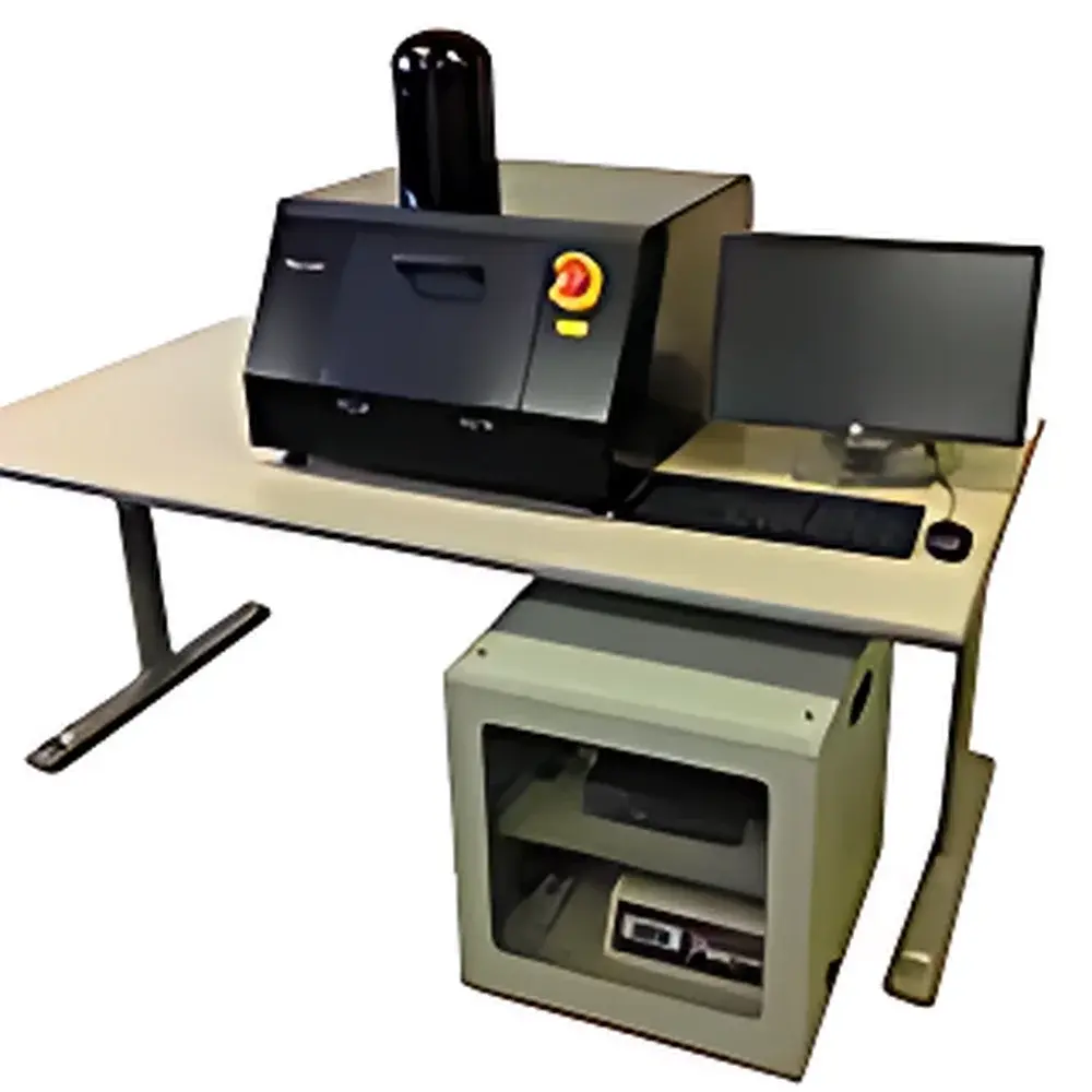
Photonic Lattice PA-110-T Full-Field Birefringence Stress Analyzer
| Brand | Photonic Lattice |
|---|---|
| Origin | Japan |
| Model | PA-110-T |
| Measurement Range | 0–130 nm |
| Repeatability | < 1.0 nm |
| Pixel Resolution | 1120 × 868 |
| Measurement Wavelength | 520 nm |
| Maximum Sample Area | 8-inch diameter |
| Dimensions | 650 × 700 × 683 mm |
| Weight | 70 kg |
| Data Interface | Gigabit Ethernet (camera), RS-232C |
| Power Supply | AC 100–240 V, 50/60 Hz |
| Software | PA-View, PA-Rasterscan |
Overview
The Photonic Lattice PA-110-T is a full-field, quantitative birefringence stress analyzer engineered for high-precision, non-contact evaluation of internal stress and optical anisotropy in transparent crystalline and polymeric materials. It operates on the principle of photoelasticity: when linearly polarized light propagates through a stressed transparent medium, the induced birefringence splits the incident beam into two orthogonal polarization components with a relative phase delay (retardation), directly proportional to the local stress magnitude and orientation. The PA-110-T captures this spatially resolved retardation distribution across the entire sample surface—up to 8-inch wafers—in a single, calibrated measurement cycle. Unlike conventional crossed-polarizer visual inspection, which yields only qualitative defect detection, the PA-110-T delivers traceable, numerical retardation maps (in nanometers) with sub-nanometer repeatability (<1.0 nm), enabling objective process control and statistical analysis of stress-induced crystal lattice distortion in sapphire, SiC, fused silica, and advanced optical glasses.
Key Features
- Full-field, high-resolution retardation imaging using a proprietary photonic-crystal-based polarization sensor—capable of simultaneous acquisition of all four Stokes parameters at 520 nm wavelength.
- Automated XY scanning stage with raster-scan stitching functionality, supporting seamless metrology of large-area substrates (e.g., 200 mm wafers) without manual repositioning or operator intervention.
- Large-aperture telecentric optical path ensures uniform illumination and minimal perspective distortion, enabling accurate measurement within ±1 mm of wafer edge—critical for edge-sensitive semiconductor and LED substrate applications.
- Integrated real-time data acquisition and processing engine, delivering complete 2D retardation maps in under 5 minutes for an 8-inch wafer—significantly faster than point-scanning interferometric or ellipsometric alternatives.
- Rugged industrial-grade mechanical architecture (70 kg mass, vibration-damped base) designed for integration into cleanroom environments and production-line metrology stations.
Sample Compatibility & Compliance
The PA-110-T is validated for use with optically transparent, isotropic-to-anisotropic transition materials including sapphire (Al₂O₃), silicon carbide (SiC), quartz, BK7 glass, PMMA, polycarbonate, and spin-coated optical films. It supports both free-standing wafers and bonded substrates mounted on standard SEM/inspection carriers. Measurement results are traceable to NIST-traceable polarization standards and comply with key industry protocols for optical stress qualification—including ASTM F2629 (Standard Practice for Measuring Residual Stress in Transparent Materials Using Photoelasticity), ISO 11146 (Laser Beam Parameters), and JEDEC JESD22-A112 (Mechanical Stress Testing of Semiconductor Devices). The system’s deterministic calibration routine satisfies GLP/GMP documentation requirements, and raw image data includes embedded metadata (timestamp, exposure, stage coordinates, calibration ID) to support FDA 21 CFR Part 11 audit trails when used with validated PA-View software configurations.
Software & Data Management
PA-View and PA-Rasterscan constitute the certified software suite for instrument control, image acquisition, and quantitative analysis. PA-View provides real-time visualization of retardation magnitude and fast-axis orientation vectors; it supports ISO-standard file export (TIFF, CSV, HDF5) and batch processing of multi-wafer datasets. PA-Rasterscan enables automated mosaic acquisition with sub-pixel registration accuracy (<0.5 µm), geometric correction for lens distortion, and region-of-interest (ROI) masking for yield analysis. Both applications implement role-based user access controls, electronic signature logging, and change history tracking—fully compatible with laboratory information management systems (LIMS) via RESTful API. All processed data files retain cryptographic hash signatures to ensure data integrity during archival or regulatory submission.
Applications
- Quantitative mapping of residual stress gradients in sapphire and SiC wafers post-lapping, polishing, or epitaxial growth—correlating stress hotspots with downstream cracking or device failure rates.
- In-line monitoring of thermal stress development during annealing or bonding processes in micro-LED and power electronics manufacturing.
- Characterization of birefringence uniformity in optical lens blanks, prisms, and laser cavity windows to meet MIL-PRF-13830B scratch-dig and wavefront distortion specifications.
- Failure analysis of polymer-based optical films (AR coatings, retardation films, touch panel laminates) where localized strain induces unwanted color shifts or contrast loss.
- Research-grade validation of finite element models (FEM) simulating thermo-mechanical stress in novel transparent ceramics and metamaterial substrates.
FAQ
What physical parameter does the PA-110-T measure, and in what units?
It measures optical retardation (phase difference between orthogonal polarization components) in nanometers (nm), directly correlated to internal stress via the stress-optic coefficient of the material.
Can the system distinguish between intrinsic birefringence and stress-induced birefringence?
Yes—by combining multi-angle illumination and fast-axis orientation analysis, PA-View enables separation of form birefringence (e.g., from periodic nanostructures) from stress-induced contributions using tensor decomposition algorithms.
Is the PA-110-T suitable for measuring curved or non-planar samples?
No—it is optimized for flat, parallel-faced transparent substrates. Curved surfaces require custom optical adaptors not included in the standard configuration.
Does the system require external calibration standards for daily operation?
No—each unit ships with a factory-calibrated reference plate and performs automated self-calibration prior to every measurement sequence using built-in polarization state generators.
How is measurement uncertainty quantified and documented?
Repeatability (<1.0 nm) and spatial uncertainty (±2 µm) are validated per ISO/IEC 17025 procedures and reported in the Certificate of Conformance supplied with each instrument.


