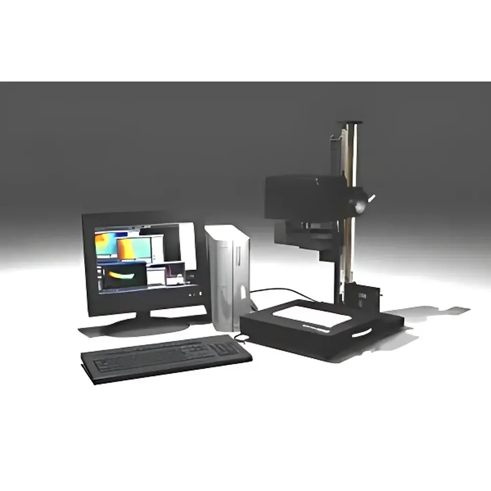
Photonic Lattice PHL PA-110-T Large-Area Birefringence Stress Analyzer
| Brand | Photonic Lattice |
|---|---|
| Origin | Japan |
| Model | PHL PA-110-T |
| Measurement Range | 0–130 nm |
| Repeatability | < 0.1 nm |
| Pixel Resolution | 1120 × 868 |
| Measurement Wavelength | 520 nm |
| Maximum Sample Diameter | 200 mm (8-inch) |
| Optical Configuration | Vertical-incidence telecentric lens |
| Data Interface | Gigabit Ethernet (camera), RS-232C |
| Software | PA-View v3.x |
| Power Supply | AC 100–240 V, 50/60 Hz |
| Dimensions | 650 × 700 × 683 mm |
| Weight | 70 kg |
Overview
The Photonic Lattice PHL PA-110-T is a high-precision, large-area birefringence stress analyzer engineered for quantitative, non-contact evaluation of optical anisotropy in transparent crystalline and polymeric materials. It operates on the principle of photoelasticity: when linearly polarized light traverses a stressed or inherently birefringent medium, its polarization state undergoes retardation—proportional to the local phase difference (δ) between orthogonal eigenmodes. By capturing full-field polarization images with a proprietary photonic-crystal-based polarization sensor, the PA-110-T reconstructs spatially resolved retardation maps (in nanometers) across substrates up to 200 mm in diameter. Unlike conventional crossed-polarizer visual inspection, this system delivers traceable, metrologically validated birefringence data—enabling correlation between internal stress distribution, crystal lattice distortion, and functional device performance in sapphire, SiC, quartz, fused silica, and advanced optical polymers.
Key Features
- Large-format measurement capability: Full-field birefringence mapping on wafers up to 200 mm (8-inch) diameter with sub-nanometer repeatability (< 0.1 nm)
- Vertical-incidence telecentric optical path: Eliminates perspective distortion and ensures uniform magnification across edge and center regions—critical for wafer-edge defect characterization
- Integrated XY motorized stage with auto-stitching: Enables seamless mosaic acquisition and geometrically corrected image synthesis for oversized samples or multi-wafer batches
- Proprietary photonic-crystal polarization imaging sensor: Captures four polarization states simultaneously at 520 nm, enabling real-time retardation calculation without mechanical rotation or sequential filtering
- PA-View software suite: Provides ISO/IEC 17025-aligned data processing—including vector field analysis, principal axis orientation mapping, stress tensor estimation (via stress-optic coefficient calibration), and statistical process control (SPC) charting
Sample Compatibility & Compliance
The PA-110-T is optimized for planar, optically transparent substrates with thicknesses ranging from 0.1 mm to 25 mm. Validated applications include sapphire and silicon carbide (SiC) wafers used in LED epitaxy and power electronics; fused silica masks for EUV lithography; tempered glass displays; and injection-molded polymer optics. The system complies with ISO 11146-1 (laser beam profiling standards, adapted for polarization metrology), ASTM E2902-21 (standard guide for birefringence measurement in optical materials), and supports audit-ready documentation per GLP and GMP requirements. Raw image data and processed retardation maps are stored with embedded metadata (timestamp, operator ID, calibration certificate ID, environmental conditions), satisfying FDA 21 CFR Part 11 electronic record integrity criteria when deployed with network authentication and role-based access control.
Software & Data Management
PA-View v3.x serves as the central analytical engine—combining acquisition, visualization, and metrological reporting in a single interface. It implements pixel-level calibration using NIST-traceable retardation standards and supports user-defined stress-optic coefficients (e.g., C = 2.8 × 10⁻¹² Pa⁻¹ for sapphire). Data export options include TIFF (16-bit signed), CSV (retardation + azimuth angle per pixel), and HDF5 (for integration with Python-based analytics pipelines). Batch processing mode enables automated analysis of production lots, generating summary reports with pass/fail thresholds, histogram distributions, and spatial trend overlays. Audit trails log all parameter modifications, software updates, and calibration events—with immutable timestamps and digital signatures.
Applications
- Crystal defect screening in sapphire and SiC wafers: Quantifying dislocation density gradients and slip band formation via localized retardation anomalies
- Residual stress mapping in tempered glass: Verifying uniformity of compressive surface stress and detecting thermal shock-induced microcracks
- Process validation for wafer bonding: Identifying interfacial stress accumulation at dielectric or metal interfaces prior to dicing
- Quality assurance of optical lenses and prisms: Detecting molding-induced birefringence in acrylic, polycarbonate, and COC substrates
- R&D of photonic integrated circuits: Characterizing stress-induced modal birefringence in silicon nitride waveguides and lithium niobate modulators
FAQ
What is the minimum detectable retardation and how is it verified?
The system achieves a noise-equivalent retardation (NER) of ≤ 0.05 nm under standard operating conditions. Verification is performed using calibrated quartz wedge standards traceable to NIST SRM 2085, with uncertainty budgets documented per ISO/IEC 17025 Annex A.
Can the PA-110-T measure birefringence in curved or non-planar samples?
No—it requires flat, parallel-surface specimens within ±10 µm flatness tolerance over the measured area. Curved substrates must be characterized using alternative methods such as point-scanning interferometric polarimetry.
Is the 520 nm wavelength fixed, or can other wavelengths be selected?
The optical head is factory-optimized for 520 nm illumination. Multi-wavelength operation (e.g., 450/520/630 nm) is supported only on the WPA-series systems; the PA-110-T is a single-wavelength configuration designed for high-speed, production-grade throughput.
How does the system handle temperature drift during long-duration measurements?
Internal thermal stabilization maintains sensor and optical path temperature within ±0.2 °C. Drift compensation algorithms reference dark-frame baselines acquired before each scan sequence, ensuring measurement stability over 8-hour continuous operation.
Does PA-View support custom scripting or API integration?
Yes—PA-View exposes a COM-based automation interface compatible with MATLAB, LabVIEW, and Python (via pywin32), enabling integration into automated test platforms and MES/SCADA environments.


