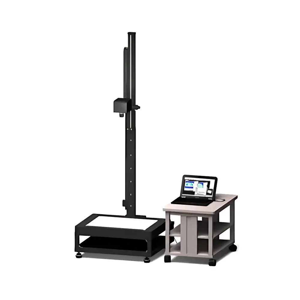
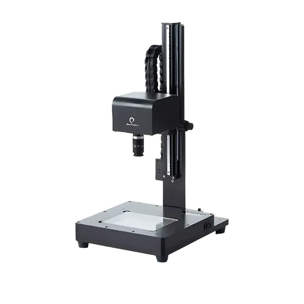
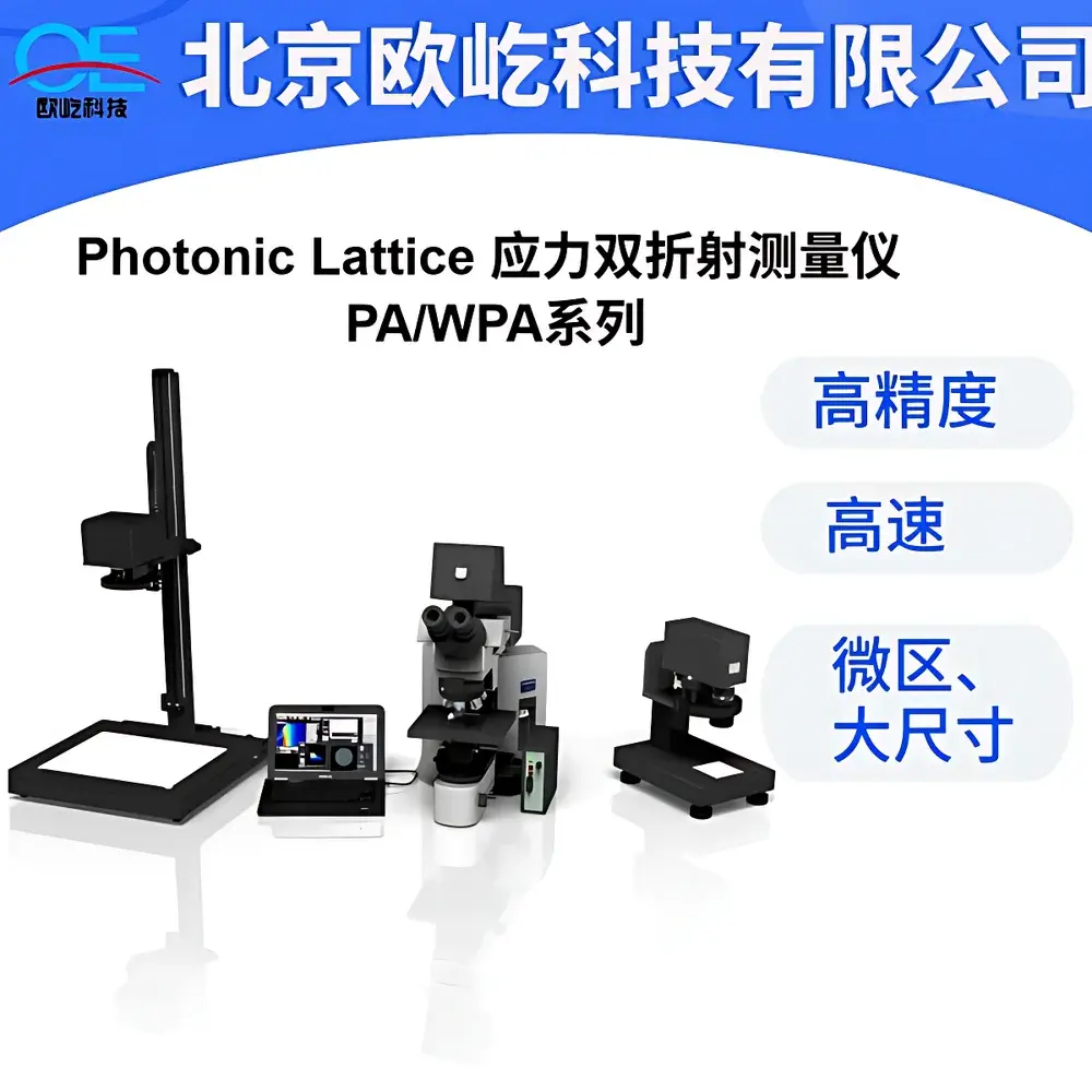
Photonic Lattice PA-300-XL SIC Polarizing Stress Meter
| Brand | Photonic Lattice |
|---|---|
| Origin | Japan |
| Model | PA-300-XL SIC |
| Output Parameters | Retardation [nm], Fast Axis Orientation [°], Stress Conversion [MPa] (optional) |
| Measurement Wavelength | 520 nm |
| Birefringence Range | 0–130 nm |
| Minimum Resolution | 0.001 nm |
| Repeatability | < 0.1 nm (σ) |
| Field of View | 40 × 48 mm to 246 × 320 mm (standard) |
| Camera Resolution | 2056 × 2464 pixels |
| Optional Features | Real-time analysis software, lens-specific analysis module, external control interface, stress-mapping data processing suite |
Overview
The Photonic Lattice PA-300-XL SIC Polarizing Stress Meter is a high-resolution, full-field birefringence measurement system engineered for quantitative evaluation of residual stress and optical anisotropy in transparent, optically active materials—particularly silicon carbide (SiC) wafers and sapphire substrates used in high-power electronics, LED fabrication, and advanced optics manufacturing. Unlike conventional point-scanning or rotating-element polarimeters, the PA-300-XL SIC employs a fixed-polarization, dual-camera imaging architecture based on photoelasticity principles and calibrated Stokes vector analysis. It captures spatially resolved retardation (δ) and fast-axis orientation (θ) maps simultaneously across the entire field of view at 520 nm illumination, eliminating mechanical motion artifacts and enabling sub-millisecond per-frame acquisition. Its design specifically addresses the challenges posed by low-birefringence, high-refractive-index, and dichroic materials—where conventional polariscopes suffer from signal saturation, polarization crosstalk, or limited dynamic range.
Key Features
- Fixed-optics architecture with no rotating waveplates or motorized filters—ensuring long-term stability, minimal maintenance, and immunity to mechanical drift.
- High-resolution 2056 × 2464 pixel polarization-sensitive CMOS camera optimized for 520 nm monochromatic illumination, delivering >12-bit dynamic range and pixel-level retardation calibration.
- Measurement speed of ≤3 seconds per full-field map (including acquisition, computation, and visualization), supporting inline process monitoring and high-throughput wafer screening.
- Adjustable field-of-view optics covering standard ranges from 40 × 48 mm up to 246 × 320 mm—enabling seamless transition from small-diameter SiC substrates (e.g., 2-inch, 4-inch) to large-format sapphire blanks (up to 8-inch equivalent).
- Integrated stress conversion algorithm compliant with ASTM F39-22 and ISO 11477 methodologies, allowing direct output of principal stress magnitude (MPa) when material-specific stress-optic coefficients are provided.
- Real-time pixel-by-pixel birefringence mapping with auto-thresholding, defect highlighting, and region-of-interest (ROI) statistics export in CSV and HDF5 formats.
Sample Compatibility & Compliance
The PA-300-XL SIC is validated for use with single-crystal and polycrystalline transparent dielectrics exhibiting linear birefringence, including but not limited to 4H-/6H-SiC wafers, C-plane and R-plane sapphire substrates, fused silica, BK7 glass, and optical-grade polymers (e.g., PC, PMMA). Its non-contact, non-destructive measurement principle requires no surface coating, vacuum environment, or electrical contact—making it suitable for cleanroom-integrated deployment (Class 100/ISO 5 compatible). The instrument conforms to IEC 61000-6-3 (EMC emissions) and IEC 61000-6-2 (immunity), and its software architecture supports audit trail logging and user access control in accordance with FDA 21 CFR Part 11 and ISO/IEC 17025 requirements for accredited testing laboratories.
Software & Data Management
The system ships with Photonic Lattice’s proprietary PolarView™ Suite v4.x, a modular Windows-based application offering three core operational modes: Standard Mapping, Lens Analysis (for aspheric and freeform optics), and External Control (via TCP/IP or LabVIEW-compatible DLLs). All measurement data—including raw Stokes images, calibrated retardation/axis matrices, and stress-derived tensors—are stored in vendor-neutral HDF5 containers with embedded metadata (timestamp, operator ID, calibration ID, environmental conditions). The software supports batch processing, comparative overlay of multiple measurements, statistical process control (SPC) charting, and automated report generation (PDF/HTML) compliant with GLP documentation standards. Optional validation packages include IQ/OQ documentation templates and traceable NIST-calibrated reference standards.
Applications
- Residual stress profiling of SiC power device wafers post-lapping, polishing, or epitaxial growth to identify edge-induced cracking risks and optimize CMP parameters.
- Quality assurance of sapphire watch crystals and optical windows for aerospace applications—detecting subsurface damage, thermal gradient effects, and crystallographic domain misalignment.
- Process development support for heteroepitaxial growth systems, where interfacial strain mapping informs buffer layer design and lattice-matching strategies.
- Failure analysis of bonded wafer stacks (e.g., SiC-on-insulator), quantifying stress accumulation at bonding interfaces under thermal cycling.
- R&D validation of anti-reflective and stress-compensating thin-film coatings on high-birefringence substrates.
FAQ
What materials can be measured with the PA-300-XL SIC?
It is optimized for transparent crystalline and amorphous dielectrics with refractive indices between 1.5 and 2.7, including SiC, sapphire, quartz, fused silica, optical glasses, and select thermoplastics.
Is calibration required before each measurement?
No—factory calibration is stable for ≥12 months under normal lab conditions; optional annual recalibration using NIST-traceable retardation standards is recommended for GMP environments.
Can the system integrate with automated wafer handling platforms?
Yes—via Ethernet-based external control API, supporting trigger synchronization, position registration, and pass/fail decision logic for integration into SECS/GEM-compliant fabs.
Does the software support multi-user role-based access control?
Yes—administrator, operator, and viewer roles with password protection, session logging, and electronic signature capability per 21 CFR Part 11 Annex 11 guidelines.
What is the minimum measurable retardation and its uncertainty?
0.001 nm resolution with repeatability better than ±0.1 nm (1σ) across the full 0–130 nm range, verified using quarter-wave and half-wave reference plates.


