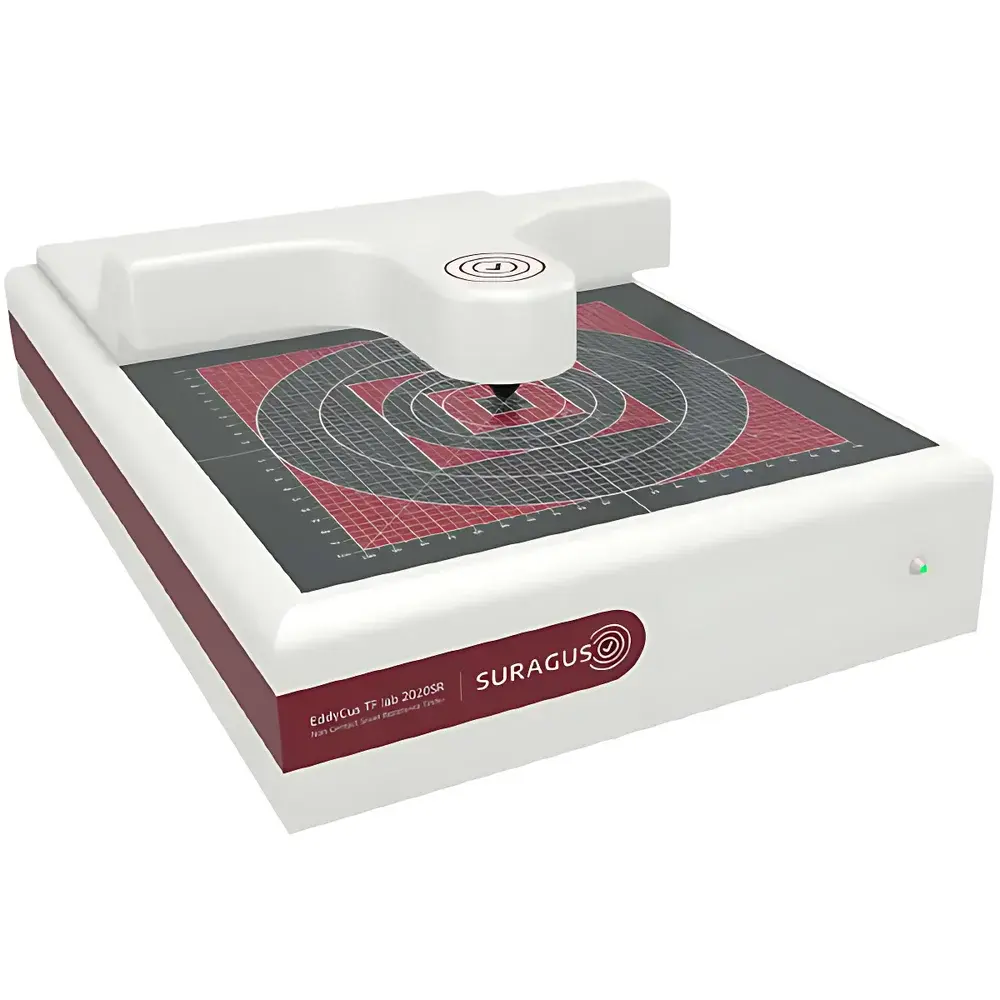
SURAGUS EddyCus TF lab 2020 Non-Contact Thin-Film Resistivity and Thickness Measurement System
| Brand | SURAGUS |
|---|---|
| Origin | Germany |
| Model | EddyCus TF lab 2020 |
| Measurement Principle | Eddy Current-Based Non-Contact Resistivity & Thickness Profiling |
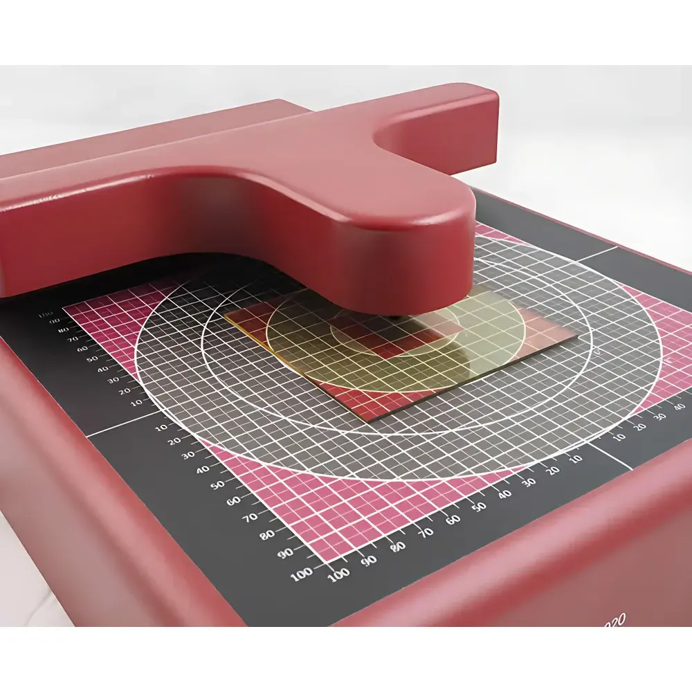
| Sample Platform | Open-Frame 204 × 204 mm (8-inch compatible) |
| Resistivity Range | 0.0001–100,000 Ω/□ (3 accuracy tiers: ±1–5% for low/mid range |
| Thickness Range (e.g., Cu) | 2 nm – 2 mm |
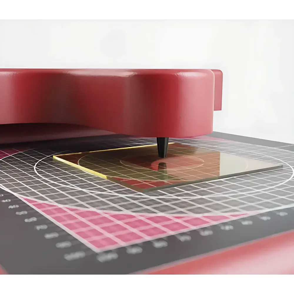
| Sensor Gap Options | 1 / 2 / 5 / 10 / 25 mm |
| Dimensions (W×D×H) | 290 × 445 × 140 mm |
| Weight | 10 kg |
| Compliance | Designed for ISO/IEC 17025-aligned lab environments |
Overview
The SURAGUS EddyCus TF lab 2020 is a precision-engineered, non-contact eddy current measurement system designed for laboratory-scale characterization of electrical sheet resistance (Rs, in Ω/□) and conductive thin-film thickness (in nm or µm). It operates on the physical principle of electromagnetic induction: a high-frequency alternating magnetic field generated by a miniature coil sensor induces eddy currents in conductive layers; the resulting impedance change is quantitatively correlated to both sheet resistance and film thickness—provided the material’s bulk conductivity or resistivity is known or calibrated. Unlike four-point probe methods, this technique eliminates mechanical contact, surface scratching, and probe alignment errors—making it ideal for fragile, patterned, or temperature-sensitive substrates such as ITO-coated glass, OLED anodes, or roll-to-roll printed electrodes. The system is optimized for Rs measurements across three dynamic ranges (low: 0.0001–10 Ω/□; mid: 0.01–1,000 Ω/□; high: 10–100,000 Ω/□), with corresponding accuracy specifications traceable to NIST-traceable reference standards. Its open-frame 204 × 204 mm sample stage accommodates wafers up to 8 inches, architectural glass panels, flexible PET substrates, and irregularly shaped prototypes—without requiring vacuum or environmental chamber integration.
Key Features
- True non-contact operation: No electrode contact, no substrate damage, no pressure-induced artifacts
- Multi-range eddy current sensing: Automatically selects optimal excitation frequency and signal conditioning for low-, mid-, and high-resistivity films
- Simultaneous Rs and thickness output: Delivers calibrated thickness values for metals (e.g., Cu, Al, Ni, Ag) based on user-defined conductivity or preloaded material libraries
- Manual XY mapping capability: Integrated software guides stepwise point-by-point scanning to generate 2D resistivity distribution maps—critical for uniformity assessment in R&D and incoming QC
- Modular sensor gap configuration: Interchangeable lift stages support gaps from 1 mm to 25 mm—enabling measurements on thick encapsulants, laminated stacks, or warped substrates
- Rugged benchtop architecture: Aluminum alloy frame, EMI-shielded electronics, and thermally stable oscillator circuitry ensure repeatability under ambient lab conditions (20–25°C, <60% RH)
Sample Compatibility & Compliance
The TF lab 2020 accepts a broad spectrum of conductive and semi-conductive thin-film systems deposited on dielectric or semi-insulating substrates—including but not limited to: sputtered ITO/FTO on float glass (Low-E coatings), evaporated Al/Cr grids for touch sensors, inkjet-printed Ag nanowire networks, CVD-grown graphene on SiO2/Si, PEDOT:PSS spin-coated layers, and electroplated Cu interconnects on PCBs. It is compatible with curved, textured, or multilayered samples where optical or profilometric methods fail. From a regulatory standpoint, the system supports documentation workflows aligned with ISO/IEC 17025:2017 (clause 7.7 on result reporting) and GLP requirements (21 CFR Part 58). While not FDA-certified per se, its software architecture permits full audit trail logging—including operator ID, timestamp, calibration certificate references, and raw impedance spectra—for internal quality audits and supplier qualification dossiers.
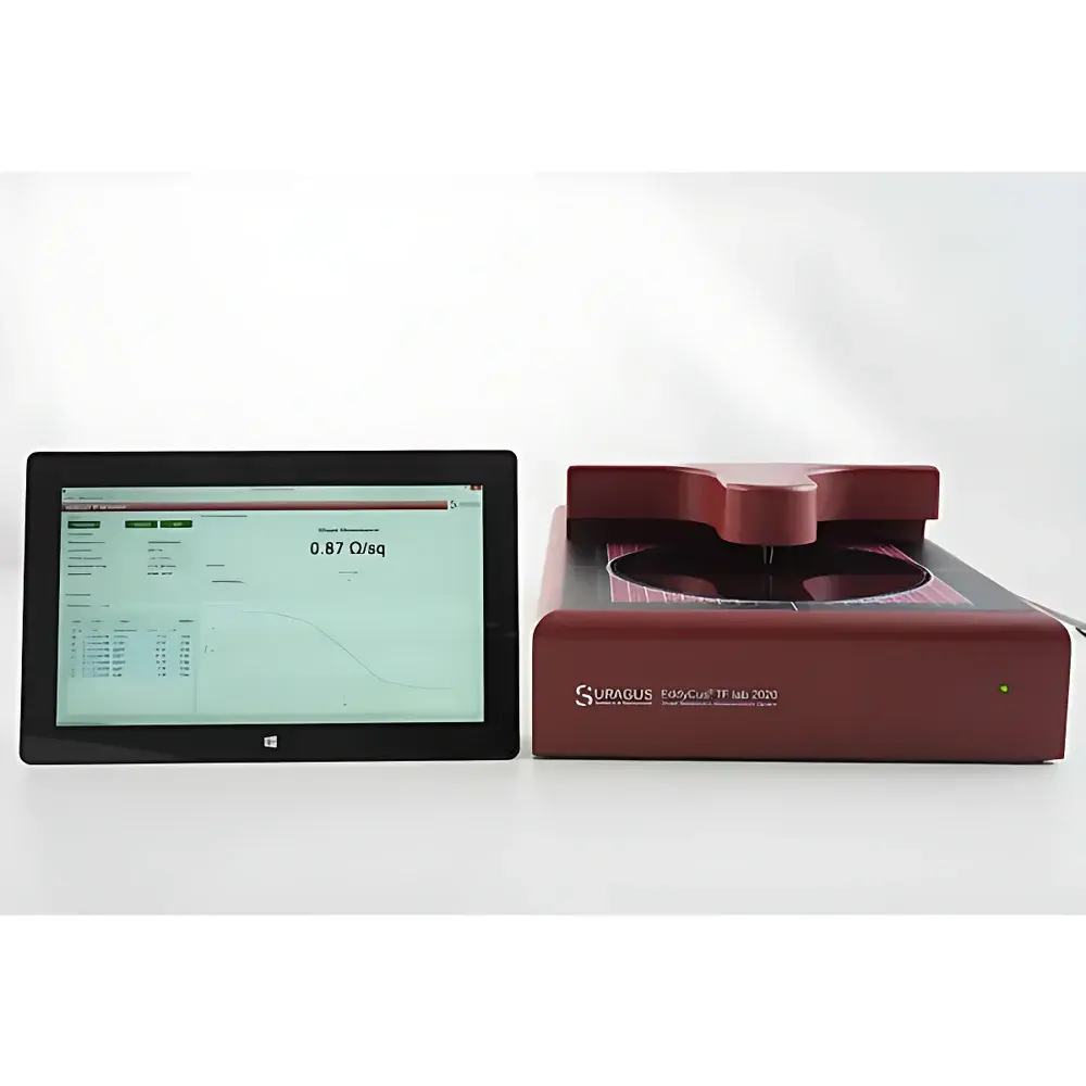
Software & Data Management
Control and analysis are executed via SURAGUS’ proprietary EddySoft v4.x platform—a Windows-based application offering intuitive wizard-driven setup, real-time impedance visualization, and batch report generation in PDF/XLSX formats. All measurement parameters (frequency, gain, offset, calibration date) are embedded in metadata. Raw data files (.edf) store full complex impedance spectra (Z′ and Z″) for post-hoc reprocessing. The software includes built-in statistical tools: Cp/Cpk calculation for process capability studies, trend charts for longitudinal monitoring, and outlier detection algorithms compliant with ASTM E29-23 (Standard Practice for Using Significant Digits in Test Data). Exported datasets conform to ASTM E1318-22 (Standard Guide for Digital Data Exchange in Materials Testing) and can be ingested into LIMS or MES platforms via CSV or OPC UA interfaces.
Applications
- Architectural glazing: Quantifying sheet resistance uniformity of Low-E coatings across 1 m² glass panes prior to lamination
- Display manufacturing: Validating Rs homogeneity of transparent electrodes in AMOLED backplanes after photolithography
- Photovoltaics: Measuring shunt resistance and finger line continuity in screen-printed Ag pastes on silicon wafers
- Flexible electronics: Characterizing bending-induced resistivity shifts in graphene/PEDOT hybrid films on PET
- Heated glass R&D: Mapping thermal uniformity correlation with local Rs variation in indium-tin-oxide heater arrays
- Advanced packaging: Verifying Cu redistribution layer (RDL) thickness consistency in fan-out wafer-level packaging (FOWLP)
FAQ
Can the TF lab 2020 measure resistivity on curved or non-planar substrates?
Yes—within mechanical limits imposed by the selected sensor gap; curvature radius must exceed 50 mm to maintain consistent lift-off distance.
Does it require periodic recalibration with certified reference standards?
Yes; SURAGUS recommends annual calibration using NIST-traceable thin-film standards (e.g., PTB-certified Si wafers with implanted P+ layers) or custom reference coupons supplied by the user.
Is thickness measurement possible for non-metallic conductors like doped metal oxides?
Yes—if the bulk conductivity (σ) or resistivity (ρ) is known or independently measured (e.g., via Hall effect), the system computes thickness using t = ρ × Rs.
Can multiple sensors be mounted for parallel multi-point acquisition?
No—the TF lab 2020 is a single-sensor, manually positioned platform; parallel mapping requires optional motorized XY stages (sold separately as EddyStage add-on).
What file formats does EddySoft support for data export and integration?
CSV (tabular results), PDF (formatted reports), XLSX (statistical summaries), and native .edf (raw impedance spectra with full metadata).


")
