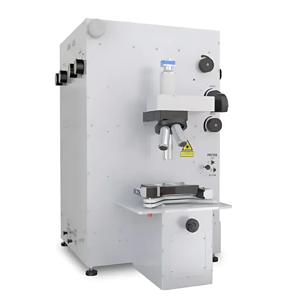
Auniontech ASOPS Imaging System – Asynchronous Optical Sampling for Picosecond Ultrasonics
| Brand | Auniontech |
|---|---|
| Origin | Imported |
| Manufacturer Type | Authorized Distributor |
| Model | ASOPS |
| Pricing | Upon Request |
Overview
The Auniontech ASOPS Imaging System is a turnkey industrial platform for non-contact, non-destructive picosecond ultrasonics based on asynchronous optical sampling (ASOPS). It leverages ultrafast laser–material interaction to generate and detect coherent acoustic phonons in the 10–100 GHz frequency range—far exceeding the resolution limits of conventional MHz–GHz scanning acoustic microscopy (SAM) or medical ultrasound. When a femtosecond pump laser pulse strikes a sample surface, absorbed energy induces transient thermoelastic expansion, launching broadband acoustic waves that propagate at ~1–10 nm/ps through thin films and multilayer structures. A time-delayed probe laser—frequency-offset from the pump by a few kHz—enables sub-picosecond temporal resolution via optical interferometric detection of surface displacement-induced reflectivity changes. This ASOPS architecture eliminates mechanical delay lines, enabling full waveform acquisition in <1 s per point. Unlike traditional zero-beat systems requiring minutes per measurement, the ASOPS system achieves high-fidelity, quantitative mapping of nanoscale mechanical and thermal properties across mm-scale areas with sub-50 µm lateral resolution and sub-nanometer axial sensitivity.
Key Features
- Patented all-optical architecture derived from CNRS and University of Bordeaux technology transfer—no coupling media, no X-rays, no physical contact, and no sample damage.
- Simultaneous multi-parameter quantification: film thickness (1 nm–30 µm), interfacial adhesion strength, nanoscale thermal boundary resistance (TBR), and in-plane thermal conductivity.
- ASOPS-enabled single-shot time-domain waveform acquisition—no moving parts, no mechanical delay stages—ensuring high reproducibility and immunity to environmental vibration.
- Compatible with opaque (metals, oxides, ceramics), semi-transparent (SiN, SiO₂), and transparent (glass, polymers) materials without coating or preparation.
- Z-axis depth resolution better than 0.5 nm; lateral resolution configurable down to 50 µm via galvo-scanning optics.
- Integrated pump-probe synchronization electronics with 1 ns time windows.
Sample Compatibility & Compliance
The system supports flat, curved, and microstructured substrates—including wafers, MEMS devices, OLED backplanes, and photovoltaic stacks—without geometric constraints. Its non-invasive nature satisfies ISO/IEC 17025 requirements for non-destructive testing (NDT) laboratories and aligns with ASTM E2984 (Standard Guide for Nondestructive Evaluation of Thin Films) and USP (Analytical Instrument Qualification). For regulated environments, data acquisition logs include timestamped metadata, user authentication, and audit trails compliant with FDA 21 CFR Part 11 when integrated with validated LIMS or ELN platforms. All optical paths are sealed and alignment-stable, meeting GLP/GMP operational robustness criteria for routine QC deployment.
Software & Data Management
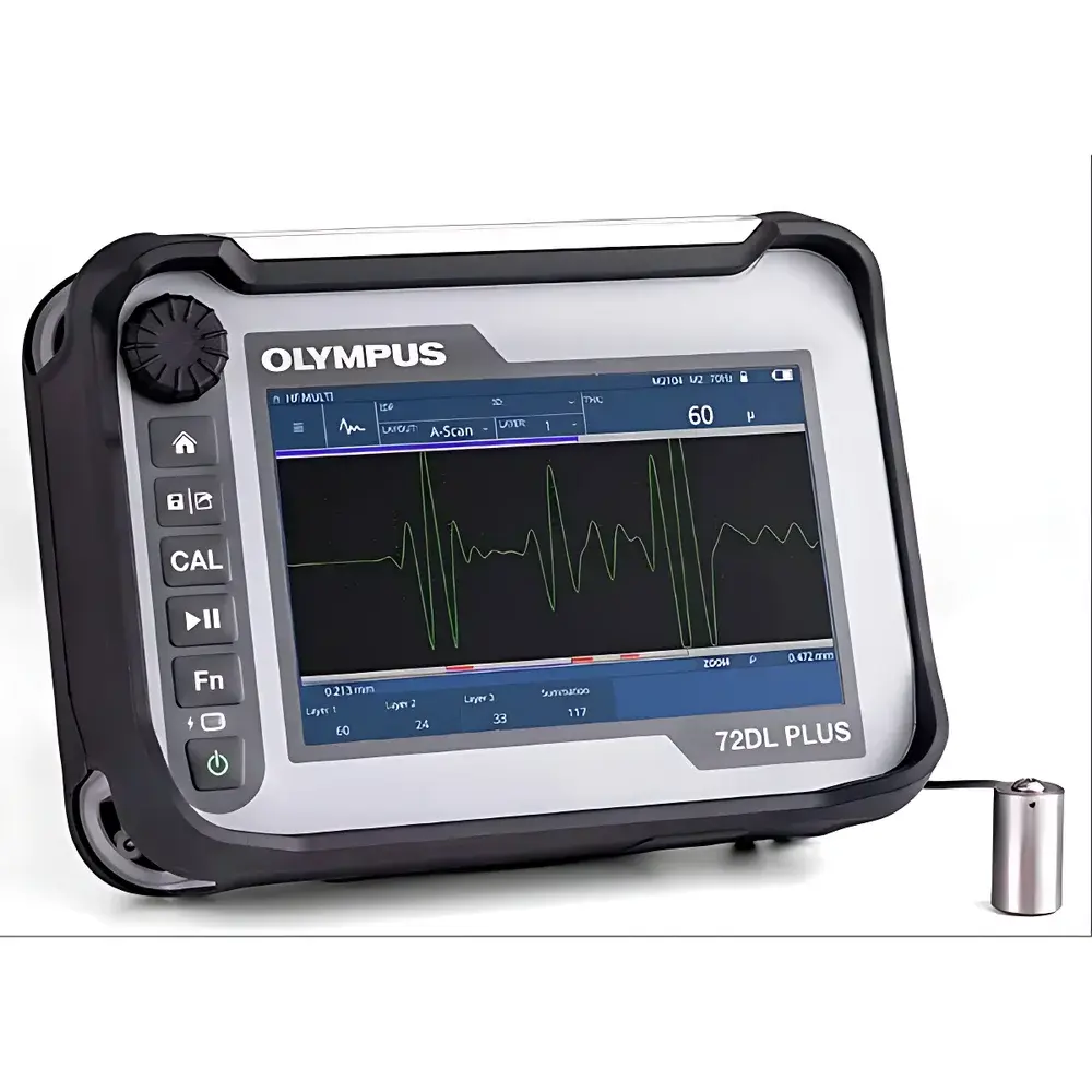
The proprietary ASOPS Control Suite provides real-time waveform visualization, automated thickness extraction, multi-layer acoustic modeling (via transfer matrix method), and inverse fitting for interface stiffness and TBR. Raw time-domain traces are stored in HDF5 format with embedded calibration parameters. Batch processing supports export to CSV, MATLAB (.mat), and industry-standard metrology formats (e.g., GDSII-compatible height maps). Software includes built-in uncertainty propagation analysis per NIST SP 960-12 guidelines and supports IQ/OQ/PQ documentation templates for instrument qualification. Remote operation and API access (Python/C++) enable integration into automated fabrication lines and SPC workflows.
Applications
- Semiconductor & Advanced Packaging: In-line thickness uniformity mapping of ALD/CVD dielectrics (<5 nm), stress-induced delamination detection in Cu/Ta/SiO₂ stacks, and TBR quantification at metal-dielectric interfaces.
- Display Manufacturing: Adhesion assessment of ITO/AgNW layers on flexible PET substrates; thickness control of quantum dot color conversion films in QLED backplanes.
- Energy Materials: Thermal conductivity profiling of thermoelectric superlattices (Bi₂Te₃/Sb₂Te₃), interfacial phonon scattering analysis in perovskite solar cell heterostructures.
- Nanomechanics Research: Surface acoustic wave (SAW) velocity imaging for local Young’s modulus extraction; picosecond phonon lifetime mapping in 2D materials (graphene, MoS₂).
- MEMS & Sensors: Residual stress mapping in released cantilevers; bonding quality verification in wafer-level encapsulation.
FAQ
What physical principles underpin ASOPS-based thickness measurement?
It relies on time-of-flight analysis of coherent acoustic echoes generated by thermoelastic expansion. The interval between successive reflections at film–substrate interfaces yields thickness with picosecond temporal precision, calibrated against known sound velocities.
Can the system characterize multilayer stacks with buried interfaces?
Yes—through forward modeling of acoustic impedance mismatches and iterative least-squares fitting of full waveforms against transfer-matrix simulations.
Is vacuum or inert atmosphere required?
No—the system operates in ambient air; acoustic damping in air is negligible at GHz frequencies due to the short propagation distances (<1 µm) involved.
How does ASOPS differ from conventional pump-probe with mechanical delay lines?
ASOPS replaces motorized stages with electronic frequency offsetting, eliminating hysteresis, wear, and vibration sensitivity—enabling faster, more stable, and higher-resolution measurements.
What sample preparation is needed?
None—optical access only is required. No metallization, polishing, or vacuum compatibility is necessary, making it suitable for post-fabrication inspection.