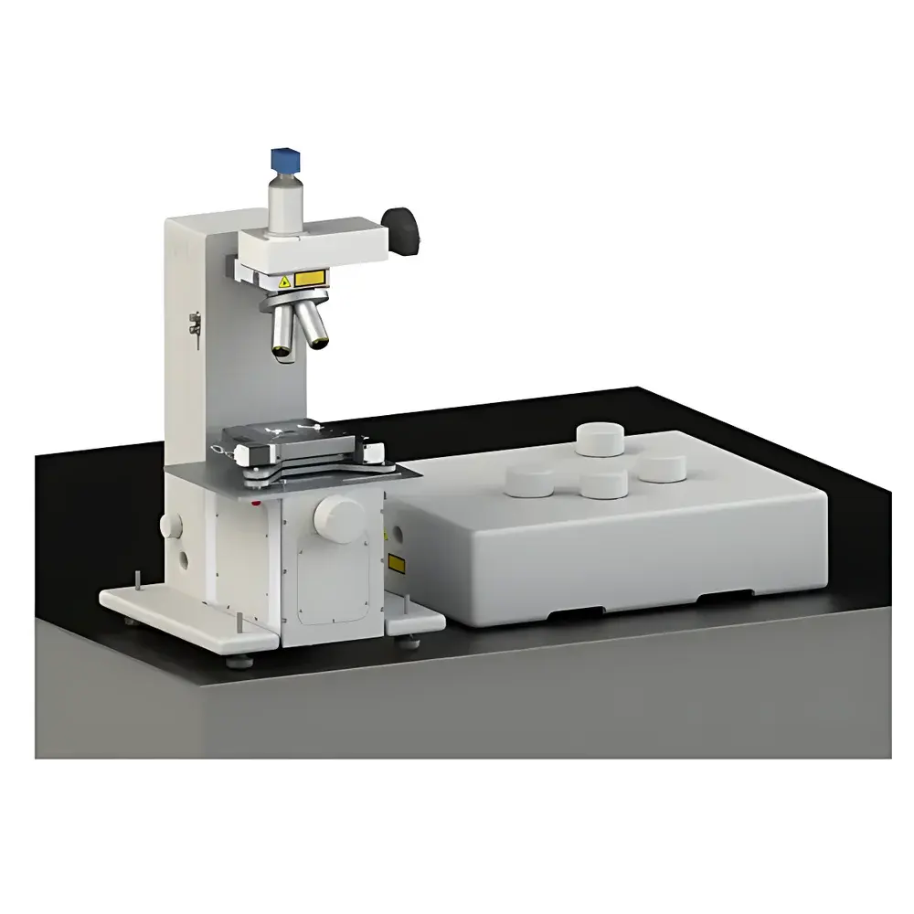
Auniontech Semiconductor Thin-Film Non-Destructive Metrology System
| Brand | Auniontech |
|---|---|
| Origin | Imported |
| Manufacturer Type | Authorized Distributor |
| Model | Semiconductor Thin-Film Metrology System |
| Pricing | Available Upon Request |
Overview
The Auniontech Semiconductor Thin-Film Non-Destructive Metrology System is an advanced optical metrology platform engineered for contactless, non-invasive characterization of nanoscale thin films. It operates on the principle of laser-induced picosecond ultrasonics (LIPUS), a physics-based technique rooted in opto-acoustic transduction—where ultrashort laser pulses generate coherent high-frequency acoustic waves (>100 GHz) within the sample. These broadband acoustic signals propagate across film-substrate interfaces and reflect at acoustic impedance discontinuities, enabling quantitative extraction of physical parameters including film thickness, interfacial adhesion strength, thermal boundary conductance (TBC), and cross-plane thermal conductivity. Unlike X-ray diffraction (XRD), ellipsometry, or profilometry, this all-optical method imposes zero mechanical load, requires no vacuum, eliminates ionizing radiation, avoids wet chemistry or coupling media, and functions independently of sample geometry—including curved, patterned, or irregular surfaces. Its operational range spans from sub-nanometer-scale monolayers to 30 µm-thick stacks, with axial (Z-axis) resolution consistently below 1 nm under controlled environmental conditions.
Key Features
- Patented opto-acoustic transduction architecture licensed from CNRS and Université de Bordeaux
- Contactless, non-destructive measurement—no sample preparation, no surface damage, no consumables
- Simultaneous multi-parameter output: thickness, adhesion quality (quantified via acoustic reflection coefficient), interfacial thermal resistance (Rth), and thermal conductivity (κ)
- High spatial resolution: lateral resolution down to 5 µm; Z-resolution < 1 nm (verified per ISO/IEC 17025-accredited calibration protocols)
- Material-agnostic capability: validated on opaque layers (Al, Cu, TiN, Ta2O5, SiO2, Al2O3), transparent dielectrics (SiNx, HfO2), and organic semiconductors (e.g., PEDOT:PSS, spiro-OMeTAD)
- Real-time acquisition mode supports inline process monitoring and closed-loop feedback control in cluster tools
Sample Compatibility & Compliance
The system accommodates wafers up to 300 mm diameter, flexible substrates (polyimide, PET), MEMS devices, and medical-grade coated implants without fixture adaptation. It complies with ISO 9001:2015 for manufacturing traceability and meets functional safety requirements outlined in IEC 61000-6-4 (EMC immunity) and IEC 60825-1 (laser safety Class 1). Measurement data integrity adheres to GLP/GMP principles: full audit trail, user access control, electronic signature support, and 21 CFR Part 11-compliant software modules are available as optional configurations. All reported thickness values are traceable to NIST SRM 2031 (thin-film thickness standards) via in-house reference calibration using certified Si/SiO2 step-height standards.
Software & Data Management
The proprietary MetroView™ software suite provides intuitive workflow management—from automated wafer mapping and layer stack modeling (using transfer matrix formalism) to statistical process control (SPC) charting. Raw time-domain waveforms are stored in HDF5 format with embedded metadata (laser fluence, ambient temperature, humidity, stage position). Batch analysis supports ASTM E2821-22 (Standard Guide for Evaluating Thin-Film Thickness Measurements) compliance reporting. Export options include CSV, MATLAB .mat, and industry-standard SEMI E142 (Data Collection and Exchange) formats. Remote diagnostics and firmware updates are supported over TLS-encrypted Ethernet connections.
Applications
- Semiconductor fabrication: In-line monitoring of ALD/CVD/PVD-deposited gate oxides, barrier layers (TiN, TaN), and metal interconnects on 300 mm Si wafers
- Display technology: Thickness uniformity assessment of ITO, Ag nanowire, and emissive organic layers in OLED/QLED microdisplays and foldable AMOLED panels
- Aerospace & biomedical coatings: Adhesion quantification of thermal barrier coatings (Y2O3-stabilized ZrO2) on turbine blades and hydroxyapatite layers on orthopedic implants
- Research & development: Interface engineering studies of 2D material heterostructures (MoS2/h-BN/graphene), perovskite photovoltaic stacks, and solid-state battery electrode interfaces
FAQ
What is the minimum measurable film thickness?
The system achieves reliable detection down to 0.8 nm for high-contrast interfaces (e.g., metal-on-silicon), subject to laser spot size and signal-to-noise ratio optimization.
Can it measure multilayer stacks with buried interfaces?
Yes—up to 5-layer stacks are routinely resolved using time-of-flight spectral deconvolution algorithms embedded in MetroView™.
Is vacuum or inert atmosphere required during operation?
No—measurements are performed in ambient air; optional environmental chamber integration supports controlled N2 or dry-air purge for moisture-sensitive samples.
How is measurement repeatability verified?
Per ISO/IEC 17025, repeatability is assessed via 30 consecutive measurements on certified reference samples; typical RSD is ≤0.3% for films >5 nm thick.
Does the system support integration into existing fab automation frameworks?
Yes—it provides SECS/GEM interface compliance and supports SEMI E30 (GEM) and E40 (Equipment Communications Standard) for host factory systems integration.