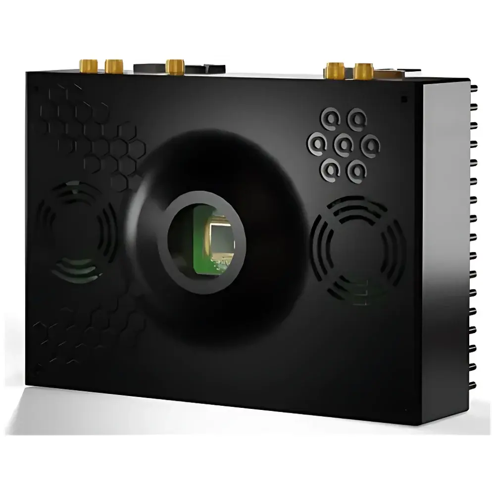
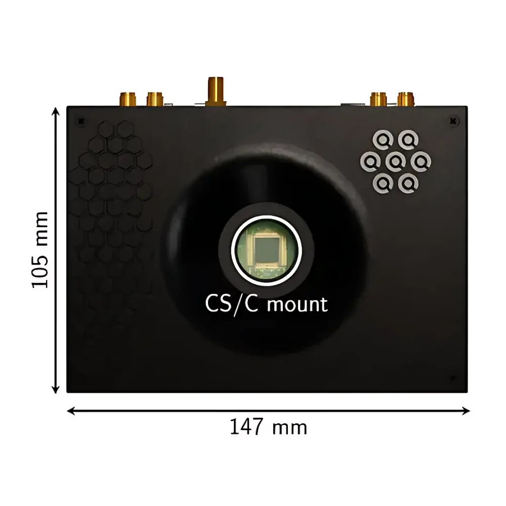
Auniontech SPAD512S Single-Photon Avalanche Diode Camera
| Brand | Auniontech |
|---|---|
| Origin | Switzerland |
| Sensor Resolution | 512 × 512 SPAD pixels |
| Peak Photon Detection Efficiency | 50% @ 520 nm |
| Dark Count Rate | 25 cps (typ.) |
| Maximum Binary Frame Rate | 97,000 fps |
| 8-bit Frame Rate | 382 fps |
| Time-Gated Imaging Resolution | 18 ps step size for gate delay tuning |
| Input Clock Support | 10/20 MHz laser sync, high-impedance, max 1.8 V |
| Power Supply | Dual 5 V USB-C or barrel-jack adapters |
| Total Power Consumption | 7.5 W (idle), up to 8.5 W (active) |
| Interface | Dual USB 3.0 (Type-B), SMA sync I/O |
| Operating Systems | Windows & Linux (SDK support for C/C++, Python) |
Overview
The Auniontech SPAD512S is a large-format, back-illuminated single-photon avalanche diode (SPAD) imaging sensor system engineered for time-resolved optical detection at the quantum limit. Developed in close collaboration with researchers from École Polytechnique Fédérale de Lausanne (EPFL), this camera implements a monolithic 512 × 512 pixel SPAD array fabricated using standard CMOS process technology—enabling scalable manufacturing while preserving high photon detection efficiency and low temporal jitter. Each pixel integrates a quenching circuit, a binary memory cell, and configurable gating logic, supporting both free-running and time-gated acquisition modes. The core measurement principle relies on time-correlated single-photon counting (TCSPC) combined with phase-resolved (phasor) lifetime analysis, where precise control over gate delay (18 ps steps) allows sub-nanosecond fluorescence decay reconstruction across the full field of view. Unlike intensified or EMCCD-based systems, the SPAD512S delivers intrinsic photon-number resolution per pixel without gain noise, making it suitable for quantitative intensity mapping, lifetime heterogeneity analysis, and quantum-optical correlation measurements.
Key Features
- Monolithic 512 × 512 SPAD array with per-pixel gating and 1-bit memory — enabling parallelized TCSPC without scanning
- Peak PDE of 50% at 520 nm, optimized for visible-range fluorophores (e.g., GFP, FITC, Rhodamine)
- Ultra-low dark count rate of 25 cps (typ.) across the array, minimized via active thermal stabilization design
- Binary frame rates up to 97 kfps; 8-bit intensity frames at 382 fps — configurable via FPGA firmware
- Hardware-level time-gating with 18 ps resolution for FLIM, LIDAR, and transient reflectance imaging
- Dual USB 3.0 (Type-B) interface for high-throughput data streaming; supports partial-readout mode (256 × 512) for increased speed
- Integrated SMA connectors for external laser clock (10/20 MHz), frame trigger, and gate synchronization — compatible with standard picosecond pulsed lasers
- Low-power architecture: 7.5 W idle, ≤8.5 W during acquisition; aluminum housing with passive heatsinking and optional forced-air cooling
Sample Compatibility & Compliance
The SPAD512S is designed for use in controlled laboratory environments including cleanrooms, optical tables, and shielded quantum optics setups. Its spectral response (350–900 nm) supports common biological fluorophores, quantum dot emitters, and near-infrared laser sources. The system complies with CE and RoHS directives for electromagnetic compatibility and hazardous substance restrictions. While not certified for clinical or GMP environments, its deterministic digital output, traceable timing architecture, and reproducible frame synchronization make it suitable for GLP-aligned research workflows. All firmware and driver binaries are timestamped and version-controlled to support auditability in regulated preclinical imaging studies. Data integrity is preserved through lossless USB 3.0 packet transmission and onboard error-checking logic within the FPGA pipeline.
Software & Data Management
Auniontech provides a cross-platform SDK supporting Windows (x64) and Linux (Ubuntu 20.04+, kernel ≥5.4). The API includes C/C++ headers, Python bindings (via ctypes), and MATLAB wrappers, enabling integration into custom acquisition pipelines, real-time processing frameworks (e.g., PyTorch-based denoising), and automated microscopy platforms. The included GUI software supports live preview, histogrammed intensity mapping, phasor plot generation, and export of raw binary frames with embedded metadata (timestamp, gate delay, exposure index). All acquired datasets conform to HDF5 format with standardized attributes aligned with the OME-NGFF specification, ensuring interoperability with ImageJ/Fiji, QuantiFluor, and openFLIM toolchains. Audit trails—including parameter changes, calibration loads, and user annotations—are logged automatically in JSON format and can be exported for regulatory documentation.
Applications
- Widefield Fluorescence Lifetime Imaging Microscopy (FLIM): Quantitative mapping of molecular interactions, metabolic state (NAD(P)H/FAD), and microenvironmental pH via multi-exponential decay fitting
- Gated Imaging: Suppression of scattered light in turbid media (e.g., tissue, aerosols), time-of-flight depth sectioning, and ballistic photon selection
- Single-Photon LiDAR: High-resolution 2D/3D topographic mapping with picosecond timing precision and ambient-light rejection
- Burst-Mode Imaging: Capturing ultrafast dynamic processes such as plasma expansion, shockwave propagation, or laser-induced breakdown
- Quantum Illumination & Non-Classical Imaging: Correlation-based target detection under extreme loss conditions using entangled or heralded photon pairs
- Time-Resolved Spectroscopy: Cross-spectral lifetime analysis in pump-probe configurations with synchronized broadband excitation
FAQ
What is the effective temporal resolution of the SPAD512S in FLIM mode?
The system achieves 18 ps gate delay resolution with hardware-defined timing accuracy of ±5 ps (RMS), enabling fluorescence lifetime discrimination down to ~100 ps with sufficient photon statistics.
Can the camera operate in continuous-wave (CW) illumination without pulsed excitation?
Yes — the SPAD512S supports free-running photon counting under CW illumination; however, lifetime extraction requires either modulated excitation or time-gated acquisition synchronized to an external source.
Is the SDK compatible with real-time GPU-accelerated processing?
The SDK exposes raw frame buffers in host memory with zero-copy access patterns, allowing direct CUDA or OpenCL memory mapping for on-the-fly deconvolution, phasor transformation, or deep learning inference.
Does the system support external triggering for synchronization with other instruments?
Yes — dedicated SMA inputs accept TTL-compatible frame triggers and laser sync signals, with programmable latency compensation up to ±1 µs in 1 ns steps.
How is calibration data stored and applied during acquisition?
Per-pixel DCR maps, PDE corrections, and timing skew profiles are stored in non-volatile memory on the sensor board and automatically loaded at initialization; users may load custom calibration files via the SDK.


