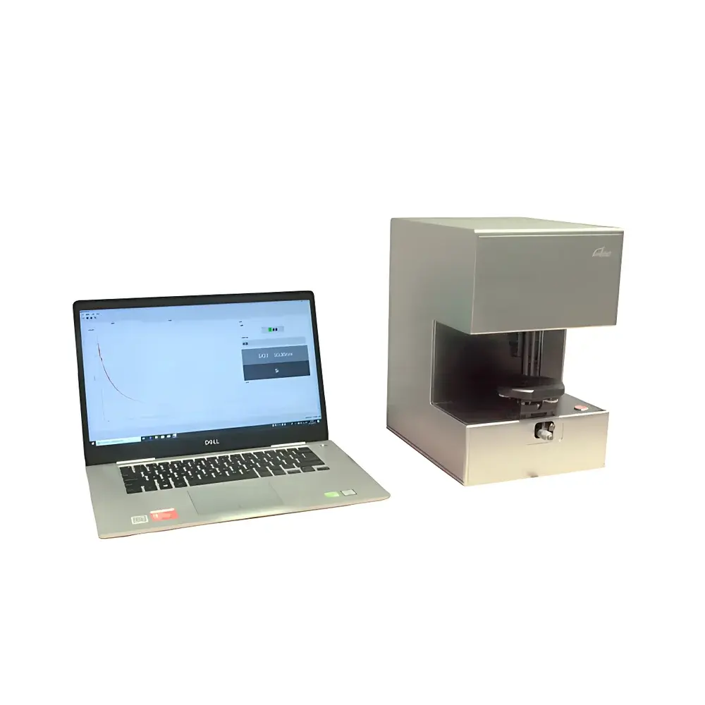
Betop Scientific Delta-VIS Online Thickness Gauge
| Brand | Betop Scientific |
|---|---|
| Origin | Guangdong, China |
| Manufacturer Type | OEM/ODM Manufacturer |
| Country of Origin | China |
| Model | Delta-VIS |
| Price Range | USD 14,000 – 28,000 |
Overview
The Betop Scientific Delta-VIS Online Thickness Gauge is a real-time, non-contact optical metrology system engineered for in-line thickness monitoring of transparent and semi-transparent thin films during continuous manufacturing processes. It operates on the principle of spectral reflectance interferometry—illuminating the sample with a broadband visible (VIS) light source (380–1050 nm), capturing the interference pattern generated by multiple internal reflections at film-substrate and air-film interfaces, and reconstructing film thickness via physics-based inverse modeling. Unlike contact profilometers or eddy-current gauges, the Delta-VIS requires no physical interaction with the substrate, eliminating risk of surface damage or process interruption. Its design prioritizes industrial robustness, thermal stability, and long-term measurement repeatability under factory-floor conditions—including ambient temperature fluctuations, vibration, and variable lighting environments. The system supports both static spot measurements and synchronized scanning across XY stages for spatial mapping, making it suitable for roll-to-roll (R2R), flat-panel, and batch-coating production lines.
Key Features
- Real-time in-line thickness monitoring with sub-nanometer resolution and ≤12 nm absolute accuracy (per ASTM E29-23 rounding rules)
- Broadband VIS illumination (380–1050 nm) optimized for high signal-to-noise ratio in oxide, polymer, and dielectric layers
- Fixed 90° normal-incidence optical geometry ensuring minimal angular sensitivity and simplified calibration traceability
- Simultaneous multi-layer analysis capability—supports up to 5-layer stack inversion with refractive index (n) and extinction coefficient (k) extraction for films >100 nm
- Modular probe architecture with optional micro-spot accessory (down to 2 mm spot diameter) for high-spatial-resolution mapping
- Integrated environmental compensation algorithms correcting for ambient temperature drift (±0.02 °C sensitivity) and mechanical stage positioning error
- Factory-calibrated against NIST-traceable SiO₂/Si reference wafers; calibration certificates compliant with ISO/IEC 17025 requirements
Sample Compatibility & Compliance
The Delta-VIS is validated for use on optically homogeneous, isotropic thin films deposited on rigid or flexible substrates—including silicon wafers, glass, PET, PI, and stainless steel. Compatible materials include SiO₂, SiNₓ, ITO, photoresists, AR/HR coatings, parylene-C, DLC, and anti-fog polymers. It meets key industry compliance frameworks: ASTM F398 (standard guide for optical thickness measurement of thin films), ISO 9277 (surface chemical analysis—XPS and AES thickness determination—comparative methodology), and supports audit-ready data integrity per FDA 21 CFR Part 11 when deployed with optional electronic signature and audit trail modules. All firmware and calibration files are digitally signed and version-controlled to ensure GLP/GMP traceability.
Software & Data Management
The Delta-VIS is operated via Betop’s proprietary ThicknessStudio™ v4.2 software—designed for integration into MES and SCADA systems via OPC UA and Modbus TCP protocols. The software provides real-time thickness trend visualization, SPC charting (X̄-R and CUSUM), automatic defect flagging based on user-defined tolerance bands, and CSV/PDF report export with embedded metadata (timestamp, operator ID, instrument serial number, calibration ID). Raw spectral data (intensity vs. wavelength) is stored in HDF5 format for third-party reanalysis. Software validation documentation (IQ/OQ/PQ templates) and 21 CFR Part 11 configuration guides are provided as standard deliverables.
Applications
- Semiconductor fabrication: In-line monitoring of gate oxides (SiO₂), passivation layers (SiNₓ), photoresist spin-coat uniformity, and SOI handle wafer thickness
- Flat-panel display: Liquid crystal cell gap control (LCD/TFT), PI alignment layer thickness, ITO electrode uniformity, and color filter stack verification
- LED & microLED manufacturing: Al₂O₃ encapsulation thickness, GaN buffer layer characterization, and phosphor film homogeneity assessment
- Automotive optics: Hard-coating (DLC, SiO₂) durability testing, anti-fog polymer layer consistency, and head-up display (HUD) waveguide thickness mapping
- Medical device coating: Parylene-C conformal coating thickness on balloon catheters, drug-eluting stent polymer layer quantification, and hydrogel film integrity screening
FAQ
Can the Delta-VIS measure opaque or metallic films?
No—it requires optical transmission or partial reflection through the film stack; fully opaque or highly absorbing layers (e.g., bulk Cu, Al) are outside its operational scope.
Is vacuum or nitrogen purge required for measurement stability?
Not required under standard factory conditions; however, an optional purged probe housing is available for environments with high humidity (>80% RH) or volatile organic contaminants.
How often does the system require recalibration?
Annual calibration is recommended per ISO/IEC 17025; field verification using certified reference standards can be performed daily or per shift.
Does it support integration with PLC-based automation systems?
Yes—native support for Siemens S7, Rockwell ControlLogix, and Beckhoff TwinCAT via EtherNet/IP and PROFINET drivers is included.
What is the minimum measurable thickness for a single-layer SiO₂ film on silicon?
1 nm (with ±1 nm uncertainty), verified per JIS K 7134 Annex B methodology using thermally grown SiO₂ reference samples.