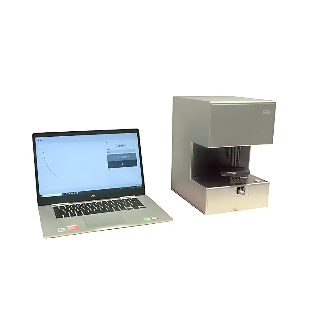
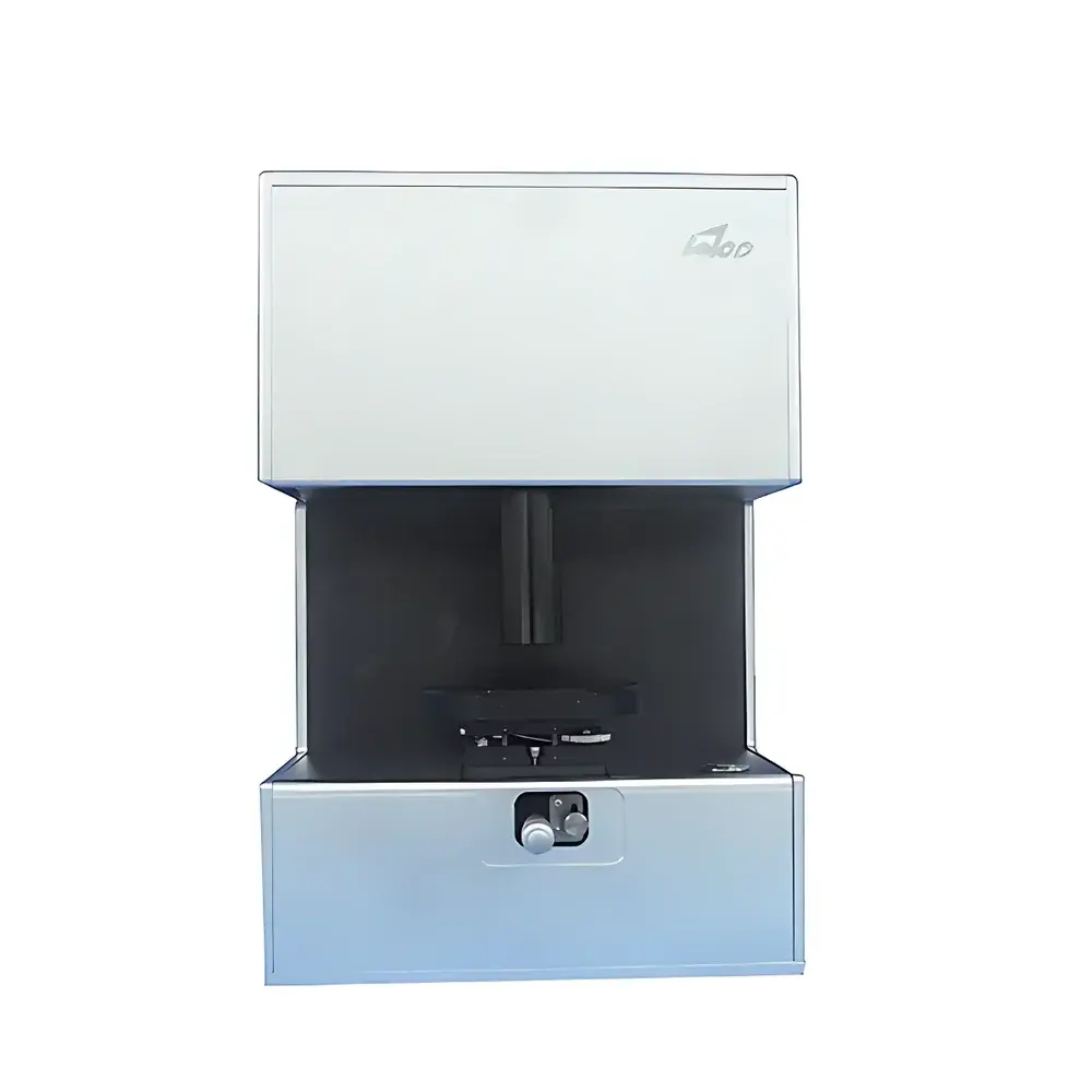
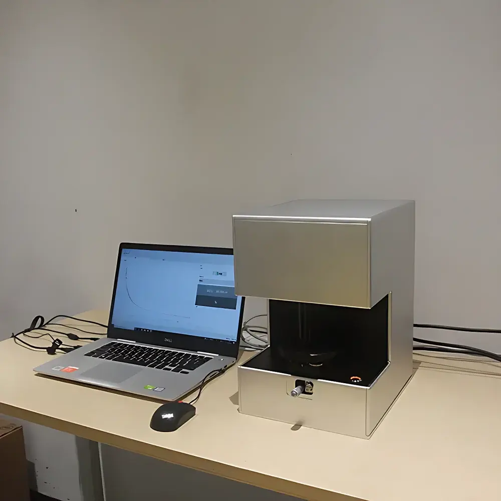
Betop Scientific Delta White Light Interferometric Thickness Measurement System
| Brand | Betop Scientific |
|---|---|
| Origin | Guangdong, China |
| Manufacturer Type | Direct Manufacturer |
| Origin Category | Domestic (China) |
| Model | Delta |
| Price Range | USD 19,500 – 56,700 (est.) |
| Wavelength Range | 380–1700 nm |
| Thickness Measurement Range | 20 nm – 3 mm |
| Thickness Accuracy | 2–10 nm |
| Measurement Modes | Reflectance & Transmittance |
| Incident Angle | 90° |
| Spot Size | 2–22 mm (configurable per optical head) |
| Multi-layer Analysis | Yes |
| Optical Constants (n & k) | Supported for films >100 nm |
| In-line Integration Capability | Yes |
| XY Scanning Option | Available |
Overview
The Betop Scientific Delta White Light Interferometric Thickness Measurement System is an engineered solution for non-contact, high-resolution optical thickness characterization of thin films and transparent/half-transparent coatings. Based on the physical principle of white light interferometry—where broadband interference fringes generated by reflection from film interfaces are spectrally resolved and analyzed—the Delta system reconstructs film thickness with nanometer-level resolution. Unlike single-wavelength ellipsometers or stylus profilers, the Delta leverages a tunable spectral acquisition architecture spanning 380–1700 nm, enabling robust measurement across diverse material systems—from sub-10-nm dielectric layers in semiconductor gate stacks to 3-mm polymer encapsulants in automotive hard coatings. Its collimated normal-incidence optical path ensures minimal angular sensitivity and eliminates alignment-induced systematic error, making it suitable for both R&D laboratories and production-integrated metrology stations.
Key Features
- Multi-spectral interferometric engine supporting three interchangeable optical heads: VIS (380–1050 nm), DUV (190–1100 nm), and XNIR (900–1700 nm), each optimized for specific thickness and material classes
- Simultaneous multi-layer thickness inversion with built-in dispersion modeling for accurate n(k) extraction on films ≥100 nm
- Sub-nanometer repeatability (≤0.2 nm RMS) and traceable accuracy (2–10 nm depending on configuration and film type)
- Non-destructive, non-contact operation compatible with fragile, temperature-sensitive, or patterned substrates
- Modular probe design with selectable spot sizes (2 mm to 22 mm) to balance spatial resolution and signal-to-noise ratio
- Factory-calibrated reference standards and NIST-traceable validation protocols included
- Integrated motorized XY scanning stage (optional) for automated mapping of thickness uniformity across wafers or display panels
Sample Compatibility & Compliance
The Delta system accommodates a broad range of optically accessible samples: transparent (e.g., fused silica, sapphire), semi-transparent (ITO, SiO₂, SiNₓ, photoresists), and layered structures (SOI, MEMS membranes, OLED stack architectures). It supports both reflectance and transmittance measurement modes, enabling analysis of front-side deposited films as well as backside or embedded layers where substrate transmission is viable. The system complies with ISO/IEC 17025 requirements for calibration traceability and supports GLP/GMP-aligned documentation workflows—including audit trails, user access control, and electronic signatures—when configured with optional FDA 21 CFR Part 11-compliant software modules. All optical components meet RoHS and CE safety directives; laser-free illumination ensures Class I eye safety per IEC 60825-1.
Software & Data Management
DeltaControl™ software provides a unified interface for instrument control, real-time spectral acquisition, model-based fitting, and statistical reporting. The platform includes preloaded optical models (Cauchy, Sellmeier, Tauc-Lorentz) and allows custom dispersion function definition. Batch processing supports automated thickness map generation with color-coded uniformity plots (±σ, CV%, min/max deviation). Raw spectral data is stored in HDF5 format for long-term archival and third-party analysis interoperability. Export options include CSV, XML, and PDF reports compliant with internal QA templates or external customer specifications (e.g., ASTM F394-22 for thin-film thickness verification). Remote monitoring and script-driven automation via Python API are supported for integration into MES or SECS/GEM environments.
Applications
- Semiconductor manufacturing: thickness and uniformity control of SiO₂, SiNₓ, low-k dielectrics, and photoresist layers on 200 mm/300 mm wafers
- Flat-panel display fabrication: liquid crystal cell gap (LCD), polyimide alignment layer, ITO electrode thickness, and AR/HR coating stack verification
- LED and micro-LED packaging: conformal passivation layers (Al₂O₃, SiO₂), phosphor film thickness, and wafer-level encapsulant uniformity
- Automotive optics: DLC, anti-fog, and anti-reflective hard coatings on polycarbonate lenses and HUD combiners
- Medical device coating: parylene-C thickness on balloon catheters, drug-eluting polymer film quantification, and stent coating integrity screening
- Research applications: 2D material monolayer verification, MOF thin-film growth kinetics, and sol-gel derived oxide film densification studies
FAQ
What optical principles does the Delta system use for thickness measurement?
It employs white light interferometry combined with spectral reflectance/transmittance analysis, resolving interference fringe envelopes across a broadband spectrum to determine optical path differences between film interfaces.
Can the Delta measure opaque or highly absorbing films?
No—it requires at least partial optical transmission or coherent reflection from internal interfaces; fully opaque metals or thick carbon-based layers fall outside its operational scope.
Is the system capable of measuring curved or non-planar substrates?
Yes, with optional auto-focus and tilt-compensation modules; standard configuration assumes flat, rigid samples within ±2° surface deviation.
How is measurement traceability maintained?
Through factory calibration using certified thickness standards (SiO₂/Si, air-gap references) and annual recalibration services aligned with ISO/IEC 17025-accredited laboratories.
Does Delta support automated integration into cleanroom fabs?
Yes—SEMI E10/E19-compliant hardware interfaces, vacuum-compatible probe variants, and FabLink™ OPC UA drivers are available upon request.