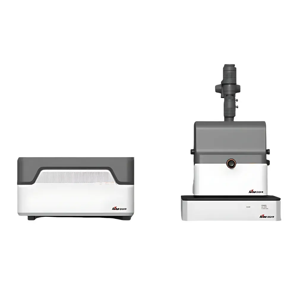
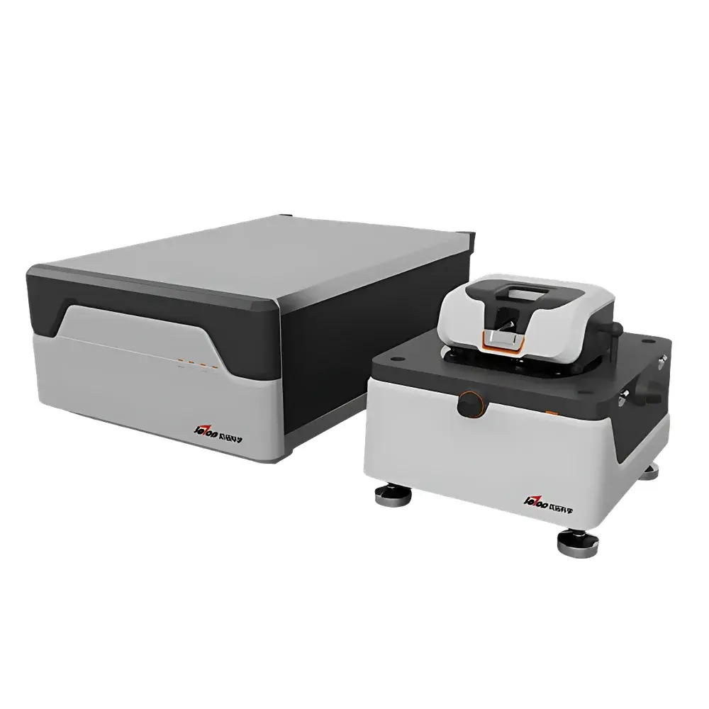
Betop Scientific OpenSPM Self-Sensing Probe Atomic Force Microscope
| Brand | Betop Scientific |
|---|---|
| Origin | Beijing, China |
| Manufacturer Type | Original Equipment Manufacturer (OEM) |
| Country of Origin | China |
| Model | OpenSPM |
| Instrument Category | Atomic Force Microscope (AFM) |
| Instrument Type | Materials Science AFM |
| Z-Direction Position Detection Noise (RMS) | ≤0.05 nm (calibrated on monolayer step height of HOPG graphite) |
| Maximum Sample Diameter | ≤30 mm |
| Maximum Sample Thickness | ≤20 mm |
| Sample Stage Travel Range (Auto-Approach) | ≥23 mm (one-click automated approach), Minimum Step Resolution: ≤50 nm |
| Manual XY Adjustment Range | ≥±8.0 mm |
| Scanner Type | Tube Scanner |
| Maximum Scan Range | ≥20 μm × 20 μm × 3 μm |
| Lateral Resolution | <0.02 nm (in-plane) |
| Scan Rate | 0.1–30 lines/sec |
| PID Feedback Loop Response Time | <10 μs |
| Max Pixel Density per Image | 4000 × 4000 physical pixels |
| Real-Time Simultaneous Data Channels | ≥5 |
| Control Architecture | Dual-Core Embedded System (ARM + DSP) |
| Communication Protocol | TCP/IP |
| Detection Mode | Frequency Modulation (FM-AFM) with Integrated Analog-Digital Lock-in Amplifier |
| Software Capabilities | Real-time 3D surface rendering, multi-parameter mapping (topography, phase, friction, current, force-distance, I–V, I–Z), tip characterization & image deconvolution algorithms |
| Compliance | Designed for GLP-compliant materials characterization workflows |
Overview
The Betop Scientific OpenSPM is a high-performance, self-sensing probe atomic force microscope engineered for precision nanoscale characterization in academic research laboratories and industrial R&D environments. Unlike conventional optical-lever-based AFMs, the OpenSPM employs a piezoresistive self-sensing cantilever architecture operating in frequency modulation (FM) mode—eliminating laser alignment complexity while maintaining sub-angstrom Z-resolution. Its core measurement principle relies on dynamic detection of cantilever resonance frequency shifts induced by tip–sample interaction forces, enabling true non-contact imaging with minimal perturbation to soft or delicate samples. The system is optimized for quantitative topographic, mechanical, electrical, and tribological property mapping across conductive, semiconductive, and insulating materials—making it particularly suited for advanced materials science, 2D material metrology, polymer morphology analysis, and nanoelectronics device inspection.
Key Features
- Self-sensing probe technology with integrated analog-digital lock-in amplifier for direct, high-bandwidth cantilever deflection readout—no external photodetector or laser alignment required.
- Dual-core embedded controller (ARM + DSP) ensures deterministic real-time feedback with PID loop response time under 10 µs, critical for stable imaging at high scan speeds and low damping conditions.
- Tubular piezoelectric scanner with ≥20 µm × 20 µm × 3 µm travel range and <0.02 nm lateral resolution, calibrated using Si(111) or HOPG atomic lattices.
- One-click automated sample approach mechanism with ≥23 mm linear travel and ≤50 nm step resolution—enabling rapid, repeatable tip positioning without manual intervention.
- Multi-modal operational flexibility: supports AFM (contact, tapping, FM), STM (for conductive surfaces), LFM (lateral force microscopy), force–distance spectroscopy, I–V and I–Z curve acquisition, and simultaneous multi-channel data collection (up to five independent signals per scan).
- Real-time 3D surface visualization engine with hardware-accelerated rendering; supports live overlay of topography, phase, friction, current, and adhesion maps during acquisition.
Sample Compatibility & Compliance
The OpenSPM accommodates standard disc-shaped specimens up to 30 mm in diameter and 20 mm in thickness, compatible with common wafer carriers and custom sample holders. Manual XY coarse positioning offers ±8.0 mm adjustment range for precise region-of-interest targeting prior to high-resolution scanning. All mechanical and electronic subsystems are designed to meet electromagnetic compatibility (EMC) requirements per IEC 61326-1 and safety standards aligned with IEC 61010-1. While not pre-certified for regulated GMP environments, the system’s embedded software architecture supports configurable audit trails, electronic signatures, and role-based user access—providing a foundation for validation under FDA 21 CFR Part 11 and ISO/IEC 17025 quality management frameworks. Calibration procedures follow traceable protocols referencing NIST-traceable HOPG step-height standards.
Software & Data Management
The OpenSPM is operated via a cross-platform desktop application built on Qt and Python-based scientific computing libraries (NumPy, SciPy, PyVista). The software implements a modular plugin architecture for extensibility and supports raw data export in HDF5 and ASCII formats—including full metadata (scan parameters, calibration constants, timestamped instrument logs). Advanced post-processing tools include tip shape estimation via blind reconstruction algorithms, convolution-based image deconvolution, quantitative roughness analysis (Sa, Sq, Sz per ISO 25178), and automated grain boundary detection. Data synchronization between acquisition and analysis modules occurs over TCP/IP, allowing remote monitoring and distributed computing integration. Optional scripting API enables automation of repetitive workflows (e.g., batch scanning, parameter sweeps, report generation) in compliance with laboratory information management system (LIMS) interfaces.
Applications
- Atomic-resolution imaging of graphene, transition metal dichalcogenides (TMDs), and other 2D layered materials.
- Quantitative nanomechanical mapping (elastic modulus, adhesion, dissipation) of polymer blends, hydrogels, and biological membranes using force spectroscopy.
- In situ electrical characterization of nanowire devices, organic transistors, and ferroelectric domains via conductive-AFM (C-AFM) and Kelvin probe force microscopy (KPFM) modes.
- Surface defect analysis and contamination assessment in semiconductor fabrication and MEMS packaging processes.
- Correlative studies combining AFM topography with Raman or fluorescence signals through external trigger synchronization (TTL-compatible I/O ports available).
FAQ
Does the OpenSPM support vacuum or liquid cell operation?
The standard configuration is optimized for ambient air and inert gas environments. Vacuum and liquid cell variants are available as optional accessories—subject to mechanical redesign of the scanner housing and environmental chamber integration.
Can third-party probes be used with the self-sensing system?
Yes—OpenSPM accepts commercially available silicon or silicon nitride cantilevers with integrated piezoresistors, provided they meet specified resistance range (1–10 kΩ) and thermal noise floor requirements. Laser-lever probes may also be mounted for comparative studies.
Is the software compatible with Windows, macOS, and Linux?
The primary acquisition and analysis software is natively supported on Windows 10/11 and Ubuntu LTS (20.04+). Command-line tools and Python API packages are platform-agnostic and tested across all three OS families.
What level of technical support is included with purchase?
All systems include lifetime remote diagnostics support, firmware updates, and access to an online knowledge base. On-site installation, training, and application-specific method development services are available under annual service agreements.