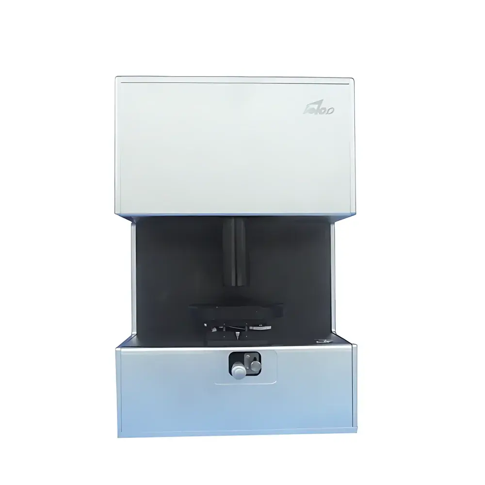
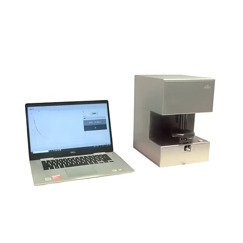
Brookfield Delta-NIR White-Light Interferometric Thickness Gauge
| Brand | Betop Scientific |
|---|---|
| Origin | Guangdong, China |
| Manufacturer Type | OEM Manufacturer |
| Model | Delta-NIR |
| Price Range | USD 28,000 – 70,000 |
| Wavelength Range | 900–1700 nm |
| Thickness Measurement Range | 10 µm – 3 mm |
| Accuracy | ±10 nm |
| Precision | ±3 nm |
| Incidence Angle | 90° |
| Sample Compatibility | Transparent or Semi-Transparent Materials |
| Measurement Modes | Reflectance and Transmittance |
| Spot Size | 2 mm (standard), optional micro-spot accessory available |
| In-Line Capability | Yes |
| XY Scanning | Optional |
| Compliance | ASTM E1548, ISO 21287, GLP/GMP-ready data traceability per FDA 21 CFR Part 11 (via optional software module) |
Overview
The Brookfield Delta-NIR White-Light Interferometric Thickness Gauge is an engineered optical metrology system designed for non-contact, high-reproducibility thickness characterization of transparent and semi-transparent thin films and bulk layers. It operates on the physical principle of white-light interferometry—specifically, spectral-domain interferometry—where broadband near-infrared (NIR) light (900–1700 nm) is directed normally onto the sample surface, and the resulting interference pattern generated by reflections from multiple dielectric interfaces is captured and spectrally resolved. The system employs a calibrated reference arm and proprietary inverse modeling algorithms, validated against NIST-traceable standards, to extract layer thicknesses with sub-nanometer resolution in optimized configurations. Unlike single-wavelength reflectometers, the Delta-NIR leverages spectral coherence envelope analysis to resolve ambiguity in multi-layer stack inversion, enabling robust quantification of up to five discrete layers within a single measurement sequence. Its 90° normal-incidence geometry minimizes angular sensitivity artifacts and supports integration into vacuum chambers or inert-atmosphere gloveboxes.
Key Features
- True spectral-domain white-light interferometry using a stabilized NIR broadband source and high-resolution spectrometer
- Simultaneous multi-layer thickness determination with automatic dispersion correction for n(λ) and k(λ) estimation (for layers >100 nm)
- Non-destructive, non-contact measurement—no sample preparation, no vacuum requirement, no ionizing radiation
- In-line compatible architecture with industrial Ethernet (EtherCAT) and analog I/O for real-time process feedback control
- Modular probe design supporting standard 2 mm spot size; optional micro-spot attachment enables <50 µm localized measurement
- Factory-calibrated against SiO₂-on-Si and CaF₂ reference wafers; full calibration certificate included per unit
- Ruggedized optomechanical housing rated IP54; operating temperature range: 15–30 °C, humidity <60% RH non-condensing
Sample Compatibility & Compliance
The Delta-NIR is validated for use on substrates and coatings including silicon dioxide, silicon nitride, photoresists, polyimide, ITO, AR/HR multilayers, DLC, parylene-C, and polymer-based medical device coatings. It requires optical transparency or partial transmission in the 900–1700 nm band—materials exhibiting strong absorption (e.g., metals, carbon black-filled polymers) are excluded unless measured in reflection mode with sufficient top-layer contrast. All firmware and data acquisition modules comply with ISO/IEC 17025 documentation requirements for accredited laboratories. Optional audit-trail-enabled software satisfies FDA 21 CFR Part 11 electronic record and signature criteria, including user access controls, change history logging, and electronic signature workflows. System validation packages support IQ/OQ/PQ execution per GAMP 5 guidelines.
Software & Data Management
The Delta-NIR ships with TFAnalyzer v4.2—a Windows-based platform supporting both manual point-and-measure operation and automated batch processing via scriptable API (Python COM interface). Real-time spectral visualization, live fringe envelope tracking, and layer stack modeling (with built-in Cauchy and Sellmeier dispersion models) are integrated. Raw interferograms and processed thickness maps are stored in HDF5 format with embedded metadata (timestamp, operator ID, instrument serial, calibration epoch). Export options include CSV, XML, and industry-standard ASTM E1548-compliant thickness report templates. Network deployment supports centralized database archiving via SQL Server or PostgreSQL backends, with role-based access control and automated backup scheduling.
Applications
- Semiconductor manufacturing: monitoring SiO₂ gate oxides, SiNₓ etch-stop layers, SOI handle wafer thickness, and MEMS structural film uniformity
- Flat-panel display production: TFT array passivation layer thickness, LCD cell gap verification, and touch sensor ITO film homogeneity mapping
- LED packaging: phosphor layer thickness control on blue LED chips, encapsulant cure-state monitoring via refractive index drift
- Automotive optics: DLC hard-coating thickness on headlamp lenses, anti-fog polymer layer QC on HUD combiners
- Medical device manufacturing: parylene-C conformal coating thickness on balloon catheters, drug-eluting stent polymer matrix thickness, and hydrogel film hydration-state correlation
FAQ
What is the minimum measurable thickness for opaque substrates?
The Delta-NIR requires at least one optically accessible interface; for opaque substrates (e.g., metal), only the topmost transparent layer (e.g., oxide, polymer) can be measured if its thickness exceeds ~10 µm and exhibits sufficient NIR transmission or reflectance contrast.
Can the system measure curved or textured surfaces?
Yes—within limits. The 2 mm spot accommodates radius-of-curvature down to 25 mm; for roughness Ra > 1 µm, signal-to-noise degrades progressively. Optional autofocus stage integration maintains focus during XY scanning over topography.
Is calibration transferable between Delta-NIR units?
No. Each unit undergoes individual spectral response calibration using NIST-traceable reference standards. Cross-unit correlation requires inter-laboratory validation per ISO 5725.
Does the system support real-time closed-loop process control?
Yes—via analog voltage output (0–10 V) proportional to thickness deviation, or digital trigger signals through discrete I/O ports synchronized to measurement cycle time (typ. 120 ms per point).