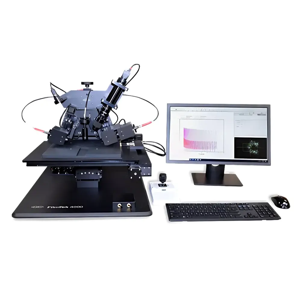
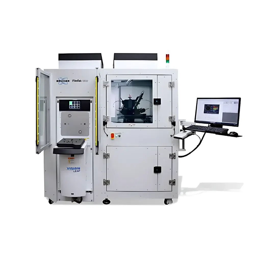
Bruker Filmtek 4000 Multi-Angle Spectroscopic Reflectometer
| Brand | Bruker |
|---|---|
| Origin | USA |
| Model | Filmtek 4000 |
| Measurement Angles | 0° (normal incidence) and 70° (grazing incidence) |
| Spectral Range | 400–1650 nm |
| Spot Size | 1 mm (0°), 2 mm (70°) |
| Thickness Range | 100 nm – 150 µm |
| Thickness Accuracy | ≤3 Å (1σ), Repeatability: ≤0.5 nm (1σ) |
| Refractive Index Resolution | 2×10⁻⁵ @ TE, 4×10⁻⁵ @ TM (1σ) |
| Stage Travel | 200 mm × 200 mm, Positioning Resolution: 1 µm |
| Light Source | Halogen lamp, Lifetime ≥2000 h |
| Detectors | Dual visible CCDs (380–950 nm, 0.3 nm resolution, 2048 px) + Dual IR InGaAs detectors (950–1650 nm, 2 nm resolution, 512 px) |
| Software | Filmtek 4000 Suite with DPSD, Cauchy, Sellmeier, Drude, Lorentz, Tauc, EMA, Graded, Superlattice, and NK modeling |
Overview
The Bruker Filmtek 4000 is a high-precision, multi-angle spectroscopic reflectometer engineered for non-contact optical characterization of thin films, thick films, and multilayer stacks in semiconductor R&D, photovoltaics, display manufacturing, and advanced materials development. Unlike conventional ellipsometers that rely on polarization state modulation, the Filmtek 4000 employs dual-angle spectral reflectance analysis—simultaneously acquiring intensity-based reflectance spectra at 0° (normal incidence) and 70° (grazing incidence) across a broad 400–1650 nm wavelength range. This dual-angle approach enables robust decoupling of thickness and complex refractive index (n + ik) without requiring prior knowledge of optical models or layer structure assumptions. The instrument operates on first-principles optical interference modeling, leveraging rigorous Fresnel equations to fit experimental spectra against physically constrained dielectric functions. Its design emphasizes metrological traceability, repeatability, and compatibility with process-integrated quality control workflows.
Key Features
- Dual-angle reflectance acquisition (0° and 70°) with independent optical paths, eliminating cross-talk and enabling simultaneous n/k extraction with minimal parameter correlation.
- High-resolution spectral detection: dual visible-range CCD spectrometers (380–950 nm, 0.3 nm resolution, 2048-pixel linear array) and dual extended-InGaAs detectors (950–1650 nm, 2 nm resolution, 512-pixel array) ensure seamless broadband coverage with calibrated radiometric response.
- Automated precision stage with 200 mm × 200 mm travel, 1 µm positioning resolution, and programmable mapping capability for full 8-inch wafer scanning—including user-defined ROI grids, line scans, and radial profiles.
- Real-time beam visualization via integrated zoom camera system, enabling precise optical alignment verification and spot placement confirmation prior to measurement.
- Intelligent optical subsystems: motorized TE/TM selector, auto-focus mechanism, and dynamic beam-centering algorithm ensure consistent illumination geometry across heterogeneous sample topographies.
- Halogen broadband source with ≥2000-hour operational lifetime and thermally stabilized output, delivering stable spectral irradiance essential for long-duration mapping and drift-sensitive applications.
Sample Compatibility & Compliance
The Filmtek 4000 accommodates substrates up to 200 mm (8-inch) diameter, including silicon wafers, glass, sapphire, flexible polymer films, and patterned OLED backplanes. Its non-contact, non-destructive methodology complies with ISO/IEC 17025 requirements for calibration laboratories and supports GLP/GMP-aligned documentation practices. All measurements adhere to ASTM F1591 (Standard Test Method for Optical Properties of Thin Films Using Spectroscopic Reflectometry) and are compatible with FDA 21 CFR Part 11-compliant software configurations when deployed with audit-trail-enabled data management modules. The system supports controlled environment integration (e.g., N₂ purge ports, temperature-stabilized stages) for hygroscopic or air-sensitive samples.
Software & Data Management
Filmtek 4000 software provides a modular, scriptable platform built on Windows 10+ with native support for SQL-based database archiving, hierarchical project organization, and role-based access control. It includes differential power spectral density (DPSD) analysis for detecting subtle interfacial roughness and compositional grading. The fitting engine implements 12 validated optical dispersion models—including Cauchy (for transparent dielectrics), Sellmeier (for wide-bandgap oxides), Drude (for metals), Lorentz oscillator (for resonant absorption), Tauc-Lorentz (for amorphous semiconductors), effective medium approximation (EMA), graded-index profiles, superlattice periodicity, and empirical NK tables. All fits generate uncertainty quantification per IUPAC guidelines, with covariance matrix reporting and residual spectrum inspection tools. Export formats include CSV, XML, HDF5, and industry-standard SE format for interoperability with third-party modeling suites.
Applications
- Process development and monitoring of ALD, PVD, and CVD-deposited films (SiO₂, SiNₓ, HfO₂, ITO, TiO₂, perovskites).
- Optical bandgap determination (Tauc analysis) and Urbach tail characterization in photovoltaic absorbers (a-Si:H, CIGS, organic PV).
- Thickness uniformity mapping of spin-coated polymer layers (photoresists, PEDOT:PSS, encapsulation films) across full wafers.
- Interfacial layer analysis in gate-stack structures (e.g., SiO₂/SiON/high-k/metal gate stacks) where conventional ellipsometry suffers from model ambiguity.
- Quality assurance of anti-reflective, high-reflection, and dichroic coatings in precision optics manufacturing.
- Research into 2D materials (MoS₂, WS₂, graphene oxide) where sub-nanometer thickness sensitivity and low-k resolution are critical.
FAQ
Does the Filmtek 4000 require vacuum or inert atmosphere operation?
No—it operates under ambient conditions; optional N₂ purge and environmental chamber interfaces are available for moisture- or oxygen-sensitive samples.
Can it measure absorbing or highly scattering films?
Yes—the dual-angle configuration and multi-model fitting engine accommodate strongly absorbing (k > 1) and turbid media by selecting appropriate dispersion relations (e.g., Tauc-Lorentz, Drude-Lorentz).
Is calibration traceable to NIST standards?
Yes—factory calibration uses NIST-traceable reference standards (Si/SiO₂ wafers, certified thickness standards); users may perform in-house verification using SRM 2030 or equivalent.
How does it handle rough or patterned surfaces?
The system integrates DPSD analysis to quantify surface/interface roughness contributions and supports effective medium modeling for patterned or nanostructured layers.
What level of technical support and training is included?
Bruker provides installation qualification (IQ), operational qualification (OQ), application-specific training, and annual preventive maintenance contracts aligned with ISO 9001 service protocols.


