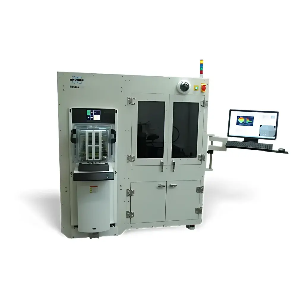
Bruker FilmTek CD Multimodal Critical Dimension and Thin-Film Ellipsometer
| Brand | Bruker |
|---|---|
| Origin | Germany |
| Model | FilmTek CD |
| Spectral Range | 190 nm – 1000 nm |
| Spot Size | 50 µm |
| Single-Measurement Time | 2 s |
| Thickness Accuracy | ±1.0 Å (NIST-traceable SiO₂ standard, 100 Å to 1 µm) |
Overview
The Bruker FilmTek CD is a high-precision, multimodal optical metrology platform engineered for simultaneous critical dimension (CD) characterization and advanced thin-film analysis in semiconductor process development and high-volume manufacturing. Unlike conventional ellipsometers or reflectometers that rely on pre-generated optical libraries and iterative regression—introducing latency and ambiguity in unknown structure analysis—the FilmTek CD implements a physics-based, library-free measurement paradigm grounded in rigorous coupled-wave analysis (RCWA). It integrates spectral generalized ellipsometry (4×4 matrix formalism), multi-angle polarized spectroscopic reflectometry (Rs, Rp, Rsp, Rps), and normal-incidence spectroscopic ellipsometry within a single optical train. This convergence enables real-time, model-independent extraction of full 3D profile parameters—including line width, sidewall angle, trench depth, pitch walk, resist height, hard mask thickness, and multi-layer stack composition—without prior structural assumptions. Designed for 1x nm node technologies and beyond, the system operates across the deep-UV to NIR spectrum (190–1000 nm), supporting both R&D and production environments with sub-nanometer thickness resolution and <10 nm CD measurement capability.
Key Features
- Multimodal optical architecture combining spectroscopic ellipsometry, polarized reflectometry, and RCWA-based diffraction modeling in one integrated platform
- Library-free, real-time optimization engine enabling rapid characterization of fully unknown nanostructures—eliminating dependence on empirical databases and reducing setup time to minutes
- 50 µm spot size with parabolic mirror optics, optimized for localized measurement on patterned wafers and small-die structures
- NIST-traceable thickness accuracy of ±1.0 Å for SiO₂ films from 100 Å to 1 µm; sub-Å repeatability demonstrated on oxide/silicon, nitride/silicon, and photoresist/silicon stacks
- Full CD parameter extraction: period, top/bottom CD, sidewall angle (SWA), groove depth, line edge roughness (LER) proxy, and profile asymmetry
- Automated wafer handling compatible with FOUP and SMIF carriers; SECS/GEM interface for factory automation integration
- Dual-source illumination: deuterium-halogen lamp (2000 h lifetime) covering 190–1000 nm with 0.3 nm spectral resolution
- 2048-pixel Sony linear CCD detector enabling high signal-to-noise ratio across DUV-NIR range
Sample Compatibility & Compliance
The FilmTek CD supports bare and patterned silicon wafers, SOI substrates, compound semiconductors (e.g., GaN, SiC), and advanced gate-stack architectures including metal gates, high-k dielectrics (HfO₂, Al₂O₃), and EUV resists. It accommodates film stacks up to 150 µm total thickness and resolves ultrathin interfacial layers (<5 Å). The system complies with ISO/IEC 17025 calibration traceability requirements through NIST-certified reference standards. Measurement data integrity adheres to FDA 21 CFR Part 11 principles via audit-trail-enabled software, electronic signatures, and secure user access controls. All firmware and analytical algorithms are validated under GLP/GMP-aligned internal protocols for use in qualification studies and process control documentation.
Software & Data Management
The proprietary FilmTek Analysis Suite features a modular, scriptable interface built on Windows 10 with multi-core CPU acceleration. Core modules include RCWA Solver, Ellipsometric Inversion Engine, Profile Fitting Workspace, and Statistical Process Control (SPC) Dashboard. Data export supports CSV, XML, and HDF5 formats; raw spectra and fit residuals are archived with metadata (timestamp, operator ID, recipe version, environmental conditions). Integration with MES platforms is enabled via OPC UA and RESTful API endpoints. Software validation packages—including IQ/OQ documentation, change control logs, and regression test reports—are available for regulated environments.
Applications
- Gate-all-around (GAA) and nanosheet transistor metrology: fin height, spacer thickness, channel oxide uniformity
- EUV lithography process monitoring: resist thickness loss, line collapse assessment, post-etch profile fidelity
- High-k/metal gate stack characterization: TiN/HfO₂/SiO₂ thickness and n/k dispersion
- Advanced packaging: redistribution layer (RDL) copper thickness, dielectric planarity, TSV barrier integrity
- MEMS and photonics fabrication: SiN waveguide cladding thickness, grating duty cycle, Bragg stack periodicity
- R&D of 2D materials: MoS₂ monolayer coverage, graphene oxide layer count, h-BN interfacial quality
FAQ
Does the FilmTek CD require optical library generation for unknown structures?
No. Its RCWA-based forward-modeling engine performs real-time, constraint-aware fitting without reliance on precomputed libraries.
Can it measure sidewall angles on sub-10 nm trenches?
Yes—profile sensitivity down to ±0.2° is achievable for trenches ≥8 nm wide using multi-angle polarized reflectometry combined with ellipsometric constraints.
Is the system qualified for use in ISO Class 1 cleanrooms?
Yes. The base configuration meets SEMI S2/S8 safety and emissions requirements; optional vibration isolation and ESD-hardened stages support Class 1 deployment.
What level of training and support is provided for first-time users?
Bruker offers comprehensive on-site installation qualification (IQ), operator certification workshops, and application-specific method development support—with dedicated semiconductor metrology engineers available globally.
How is measurement uncertainty quantified and reported?
Each measurement includes full covariance matrix output, Monte Carlo–derived confidence intervals (1σ), and traceability statements referencing NIST SRM 2032 (SiO₂ on Si) and SRM 2033 (Si₃N₄ on Si).


