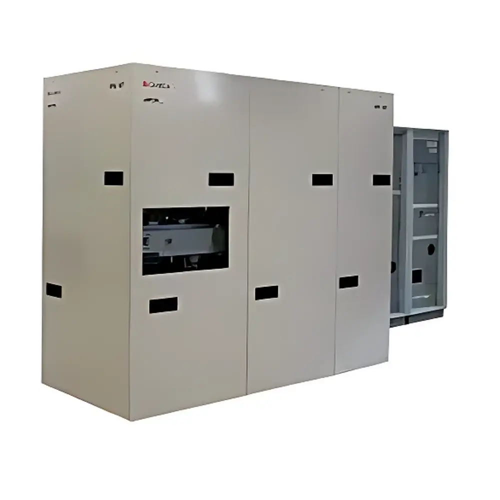
CAMECA IMS Wf and SC Ultra Secondary Ion Mass Spectrometer
| Brand | Cameca |
|---|---|
| Origin | France |
| Model | IMS Wf / SC Ultra |
| Instrument Type | Magnetic Sector Mass Spectrometer |
| Primary Beam Energy Range | 150 eV – 13 keV |
| Mass Range | 1–360 Da |
| Mass Resolution (M/ΔM) | 20,000 |
| Sample Stage Capacity | Up to 300 mm wafer (IMS Wf) |
| Automation | Fully motorized sample transfer between load lock and analysis chamber |
| Compliance | Designed for GLP/GMP-aligned semiconductor process control environments |
Overview
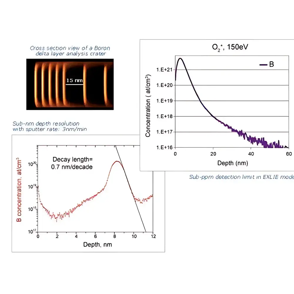
The CAMECA IMS Wf and SC Ultra are high-performance magnetic sector secondary ion mass spectrometers (SIMS) engineered for quantitative, ultra-high-resolution depth profiling in advanced semiconductor manufacturing and materials R&D. Operating on the principle of sputter-initiated ionization—where a focused primary ion beam (e.g., O−, Cs+, or O2+) bombards a solid sample surface to eject and ionize constituent atoms and molecules—the IMS Wf and SC Ultra detect ejected secondary ions with exceptional mass separation fidelity. Unlike quadrupole or time-of-flight SIMS systems, the magnetic sector architecture delivers intrinsically high mass resolution (M/ΔM = 20,000), low detection limits (sub-ppm to ppt range for dopants), and excellent isotopic fidelity—critical for metrology of ultra-shallow junctions (< 2 nm), high-k/metal gate stacks, SiGe:C:P heterostructures, and 2D materials such as graphene.
Key Features
- Ultra-broad primary beam energy range (150 eV – 13 keV), enabling optimized sputtering conditions across vastly different material systems—from ultrathin dielectrics (e.g., sub-1 nm SiOxNy) to thick epitaxial layers—without compromising mass resolution or ion transmission efficiency.
- Exclusive EXLIE (Extremely Low Impact Energy) capability down to ≤150 eV, minimizing atomic mixing and preferential sputtering artifacts during ultra-shallow depth profiling—essential for accurate quantification of B, C, N, P, and As profiles in sub-5 nm CMOS nodes.
- High-transmission magnetic sector mass analyzer with double-focusing (energy + direction) optics, ensuring stable, reproducible peak shapes and minimal mass drift over multi-hour acquisition sequences.
- Full automation architecture: motorized sample stage, robotic load-lock interface, programmable beam alignment, and closed-loop parameter synchronization—enabling unattended operation for production-level throughput and inter-lab method transferability.
- Dual-platform flexibility: IMS Wf supports full 300 mm wafer handling and up to 100 discrete samples per batch; SC Ultra emphasizes ultimate analytical sensitivity and spatial resolution for research-grade microanalysis and nano-SIMS applications.
Sample Compatibility & Compliance
The IMS Wf and SC Ultra accommodate conductive and insulating solid-state samples—including silicon wafers, compound semiconductors (GaAs, InP), oxides (HfO2, Al2O3), nitrides (SiNx), and layered 2D heterostructures—without mandatory metallization. The system integrates charge compensation via low-energy electron flood gun and variable biasing, ensuring stable secondary ion yield on insulators. Designed for semiconductor fab integration, it meets stringent environmental and operational requirements aligned with ISO 9001 quality management systems and supports audit-ready documentation for GLP and GMP workflows. While not inherently FDA 21 CFR Part 11 compliant out-of-the-box, its software architecture permits integration with validated LIMS and electronic lab notebook (ELN) platforms supporting electronic signatures and audit trails.
Software & Data Management
CAMECA’s proprietary SSW (SIMS Software Workbench) provides integrated instrument control, real-time data visualization, and post-acquisition quantification using matrix-matched standards and relative sensitivity factor (RSF) libraries. The software supports ASTM E1599 (Standard Guide for SIMS Depth Profiling) methodology templates, automated calibration routines, and batch processing of multi-sample datasets. Raw data is stored in vendor-neutral formats (e.g., .ims, .txt) compatible with third-party analysis tools including MATLAB-based profile deconvolution, PCA-driven impurity clustering, and cross-platform correlation with TEM/EELS or XPS results. All acquisition parameters—including beam current, dwell time, raster size, and energy filtering—are logged with timestamped metadata to ensure full traceability per ISO/IEC 17025 requirements.
Applications
- Quantitative dopant depth profiling in sub-3 nm FinFET and GAA transistor architectures
- Interface chemistry analysis of high-k/metal gate stacks (e.g., HfSiON/TiN, LaAlO3/Ni)
- Contamination mapping of metallic impurities (Fe, Cu, Ni) at Si/SiO2 interfaces
- Isotopic tracer studies in diffusion kinetics of Ge, C, and P in strained SiGe channels
- Depth-resolved stoichiometry of perovskite PV layers (e.g., MAPbI3) and OLED emissive stacks
- Elemental distribution in graphene/h-BN heterostructures and transition metal dichalcogenide (TMD) monolayers
FAQ
What distinguishes the IMS Wf from the SC Ultra configuration?
The IMS Wf prioritizes high-throughput wafer-scale metrology with full 300 mm compatibility and 100-sample batch loading; the SC Ultra emphasizes maximum analytical sensitivity and sub-50 nm lateral resolution for fundamental materials science investigations.
Can the system perform both positive- and negative-ion mode analysis in a single run?
Yes—via fast polarity switching (<100 ms) and independent electron flood gun control, enabling simultaneous quantification of p-type (B, Al) and n-type (P, As) dopants without re-sputtering.
Is external standardization required for quantitative SIMS?
Quantitative accuracy relies on matrix-matched reference materials (e.g., NIST SRM 2137 for Si:B). CAMECA provides certified reference standards and RSF databases traceable to SI units.
How is vacuum integrity maintained during high-throughput operation?
The system employs differential pumping with cryo-trapped turbomolecular stages and active pressure monitoring, sustaining base pressures <5×10⁻¹⁰ mbar in the analysis chamber even during continuous 300 mm wafer loading cycles.
Does the software support automated pass/fail criteria for inline process control?
SSW allows user-defined acceptance thresholds (e.g., junction depth deviation ±0.15 nm, dopant concentration tolerance ±5%) with exportable CSV reports compatible with factory MES systems.