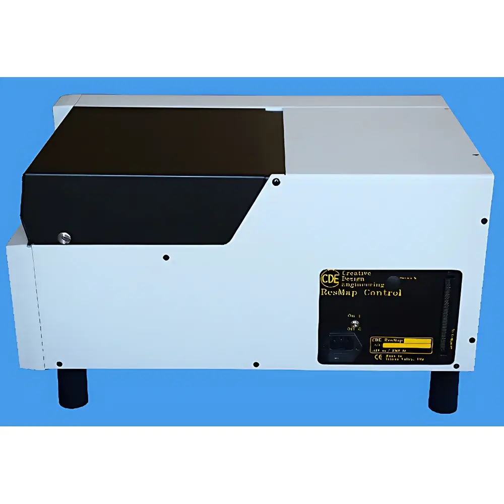
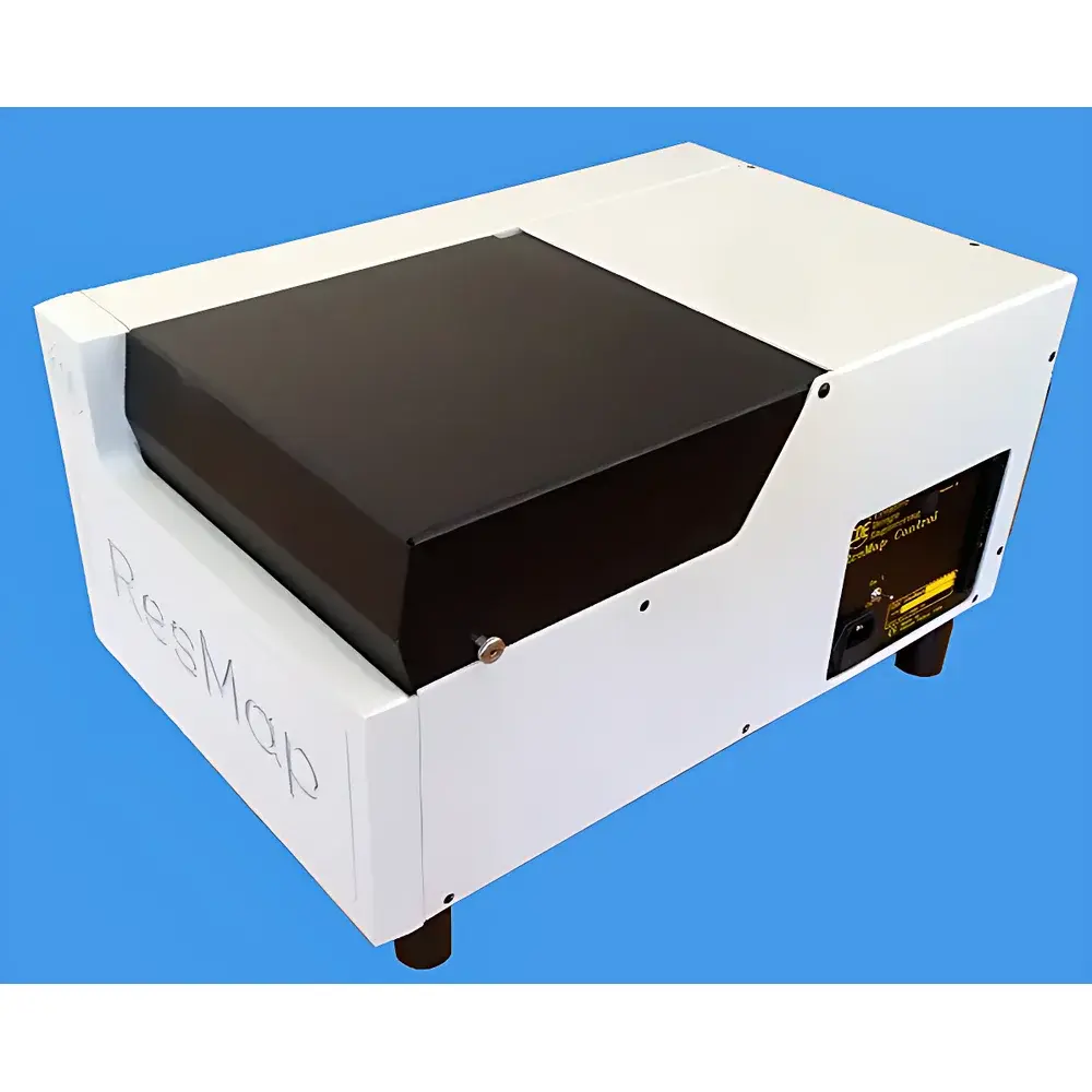
CDE ResMap 178 Four-Point Probe Sheet Resistance Mapping System
| Brand | CDE (Creative Design Engineering) |
|---|---|
| Model | ResMap 178 |
| Origin | USA |
| Automation Level | Semi-Automatic |
| Measurement Range | 1 mΩ/□ to 5 MΩ/□ |
| Repeatability | ≤ ±0.02% (on static standard resistor) |
| Scan Speed | ≥49 points/min |
| Edge Correction Capability | Effective within 1.5 mm from wafer edge |
| Probe Force Control | Software-adjustable, 90–200 g |
| Probe Types Available | A, B, K, M, N series and custom configurations |
| Supported Substrates | Circular wafers up to 200 mm (8″), square substrates up to 156 mm × 156 mm |
| Data Output | 2D/3D resistivity maps, statistical summaries, Excel-compatible reports |
| Compliance | NIST-traceable calibration standards included (6 certified reference wafers) |
Overview
The CDE ResMap 178 is a semi-automated four-point probe sheet resistance mapping system engineered for high-precision, non-destructive characterization of conductive thin films in semiconductor fabrication, photovoltaic R&D, and advanced materials laboratories. Utilizing the established four-point collinear probe method—compliant with ASTM F84 and ISO 10474—the ResMap 178 eliminates voltage drop errors associated with contact resistance by separating current injection and voltage sensing functions across four independently positioned tungsten carbide (WC) probes. This architecture ensures traceable, reproducible measurements of sheet resistance (Rs, in Ω/□), bulk resistivity (ρ, in Ω·cm), and—when combined with film thickness data—carrier concentration estimation for doped layers. Designed and manufactured by Creative Design Engineering (CDE), a Silicon Valley-based specialist founded in 1995, the ResMap 178 integrates decades of empirical optimization in probe mechanics, signal conditioning, and edge-compensated spatial algorithms. Its deployment spans >1,000 systems globally—including >24% dedicated to 300 mm process monitoring—and supports both inline quality assurance and offline research-grade metrology.
Key Features
- Sub-0.02% measurement repeatability on NIST-traceable standard resistors—validated per GLP-compliant internal audit protocols
- Programmable point-by-point scanning at ≥49 locations per minute, with full coordinate definition via intuitive Windows-based GUI
- Edge-adaptive measurement capability: reliable data acquisition within 1.5 mm of wafer or substrate perimeter, enabled by proprietary geometric correction algorithms
- Software-controlled probe force modulation (90–200 g range) with 0.01 mm vertical resolution—critical for fragile SOI, GaN, or ultra-thin Si layers
- Dual-probe head configuration with automated probe conditioning (cleaning/stroking cycle) to maintain tip geometry and minimize drift
- Modular hardware architecture: supports optional front-end integration (SEMI E47.1 compliant), auto-loader interfaces for PV production lines, and multi-head expansion (up to 4 probes on 300 mm platforms)
- Calibration traceability backed by six NIST-certified reference wafers supplied standard with each system
Sample Compatibility & Compliance
The ResMap 178 accommodates rigid planar substrates including silicon, sapphire, glass, and ceramic wafers ranging from 50 mm (2″) to 200 mm (8″) in diameter, as well as square formats up to 156 mm × 156 mm—common in solar cell manufacturing. It is routinely deployed for process control of ion-implanted junctions (Rs > 2 kΩ/□), copper metallization (Rs down to 1.67 mΩ·cm), amorphous/microcrystalline silicon absorbers, selective emitters, passivated contacts (e.g., TOPCon, POLO), and transparent conductive oxides (ITO, AZO). All measurement routines adhere to industry-standard test methodologies defined in ASTM F84 (Standard Test Method for Measuring Resistivity of Silicon Wafers with an In-Line Four-Point Probe), ISO 10474 (Semiconductor materials — Specification of silicon wafers), and SEMI MF1530 (Guide for Four-Point Probe Measurements). The system’s firmware and data logging structure support 21 CFR Part 11-compliant electronic records when configured with audit-trail-enabled software modules.
Software & Data Management
ResMap Control Suite v6.x provides a deterministic, deterministic Windows 10–compatible environment for instrument orchestration, real-time visualization, and metrological reporting. Key capabilities include: fully customizable measurement recipes (including variable step size, radial/spiral/linear scan patterns), dynamic probe pressure profiling per site, automatic outlier rejection using iterative Grubbs’ test, and export of raw voltage/current pairs alongside derived Rs values. Data output conforms to ASTM E2851 metadata schema, enabling direct ingestion into MES platforms such as Applied Materials Endura® Analytics or PDF Solutions Exensio®. Statistical summaries—Cp/Cpk, X-bar/R charts, sigma-level analysis—are generated natively; 2D color-mapped resistivity heatmaps and 3D topographic surface plots are exportable in PNG, TIFF, and CSV formats. Audit trail functionality logs all user actions, parameter changes, and calibration events with timestamp, operator ID, and digital signature—fully aligned with ISO/IEC 17025 and FDA GLP requirements.
Applications
- Process development and qualification of diffusion, implantation, and annealing steps in CMOS, MEMS, and power device fabs
- Inline monitoring of emitter sheet resistance uniformity in PERC, TOPCon, and HJT solar cell production
- Characterization of TCO layer homogeneity on large-area glass substrates for display and PV applications
- Research-grade mapping of 2D material conductivity (graphene, MoS2) and heterostructure interfacial resistance
- Failure analysis of electroplated Cu interconnects, including void detection through localized Rs deviation
- Validation of ALD/PVD-deposited barrier layers (TaN, TiN) for via-fill integrity assessment
FAQ
Does the ResMap 178 support 300 mm wafers?
No—the ResMap 178 platform is optimized for substrates up to 200 mm (8″) diameter or 156 mm square. For 300 mm applications, CDE recommends the ResMap 273 series, which includes dual/multi-probe configurations and front-end module compatibility.
Can the system measure resistivity of non-uniform or patterned films?
Yes—provided the measurement area (typically ~1 mm² under probe footprint) is locally homogeneous. The system does not resolve sub-micron features but delivers statistically representative Rs values across macroscopic regions, making it suitable for blanket film QA and process window verification.
Is probe replacement required after a specific number of measurements?
Tungsten carbide probes exhibit >500,000 measurement cycles under nominal loading conditions. Tip wear is monitored via periodic repeatability validation; replacement is recommended only upon observed degradation exceeding ±0.05% repeatability on reference standards.
How is calibration maintained between NIST standard wafer uses?
The system performs automated zero-offset compensation before each run. Long-term stability is verified quarterly using the included NIST-traceable wafers; calibration certificates are issued per ISO/IEC 17025-accredited procedures by CDE’s Metrology Lab.
Does the software support automated report generation for ISO 9001 audits?
Yes—customizable templates generate PDF reports containing measurement parameters, environmental conditions (temperature/humidity logs), operator ID, equipment ID, uncertainty budgets, and statistical process control charts—all structured to satisfy ISO 9001:2015 clause 8.5.1 requirements for documented information.


