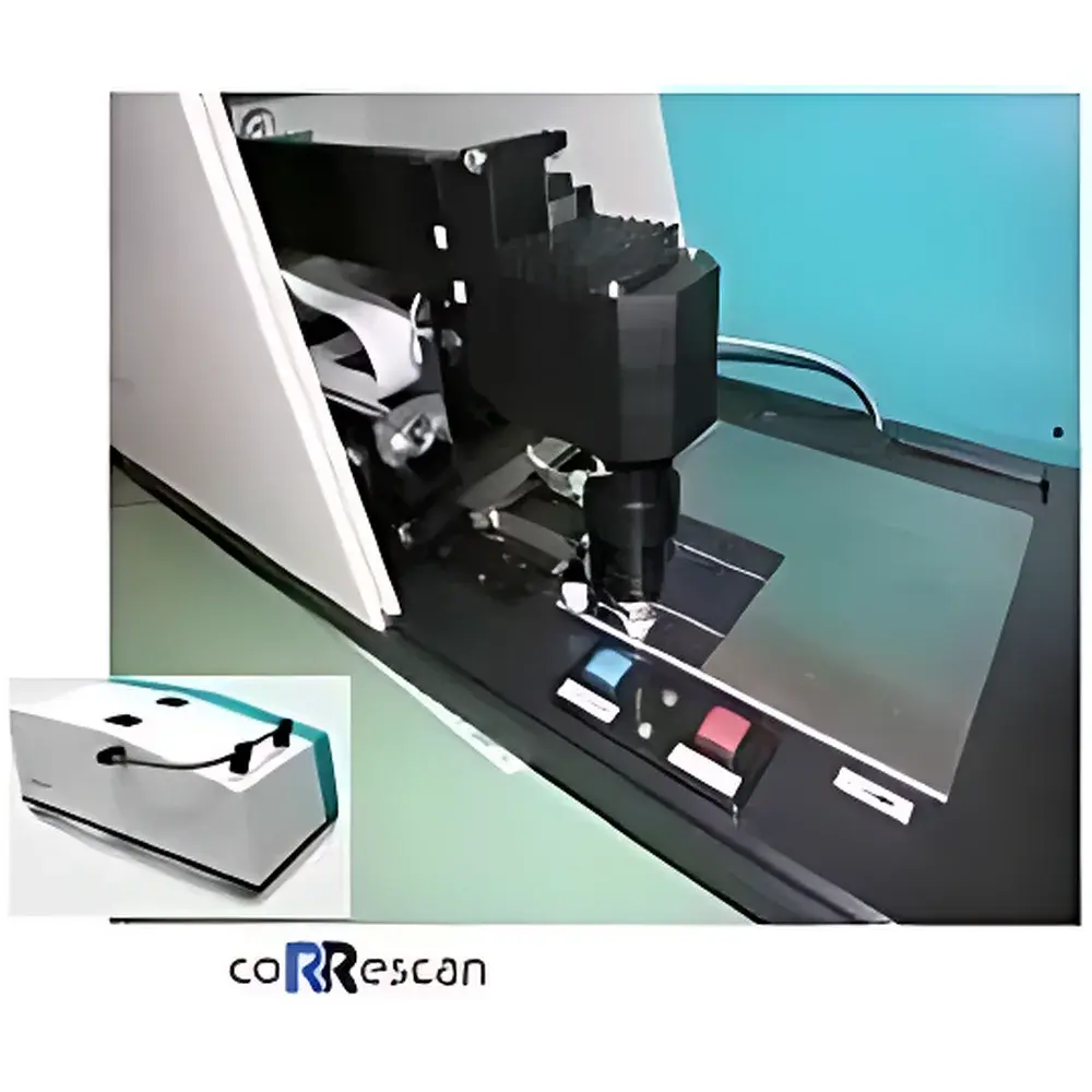
CoreScan & Sherescan Photovoltaic Wafer Sheet Resistance and Shunt Resistance Mapping System
| Origin | Netherlands |
|---|---|
| Manufacturer Type | Authorized Distributor |
| Import Status | Imported |
| Model | CoreScan / Sherescan |
| Pricing | Available Upon Request |
Overview
The CoreScan and Sherescan series are high-resolution, non-contact, optical beam-induced current (OBIC) and lock-in thermography–enabled mapping systems engineered for inline and offline characterization of silicon photovoltaic (PV) wafers and solar cells. Designed and calibrated in the Netherlands, these instruments operate on the principle of spatially resolved resistive and photovoltage response measurement—leveraging modulated infrared or visible illumination coupled with precision low-noise current/voltage sensing to generate quantitative, pixel-level maps of sheet resistance (Rs), shunt resistance (Rsh), open-circuit voltage (Voc), and light-beam-induced current (LBIC). Unlike conventional four-point probe or eddy-current methods, CoreScan and Sherescan provide full-surface, non-destructive, process-agnostic metrology—enabling root-cause analysis of metallization, diffusion, passivation, and texturing defects without physical contact or sample preparation.
Key Features
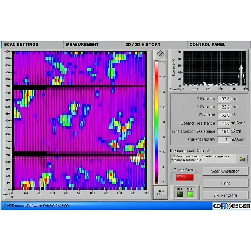
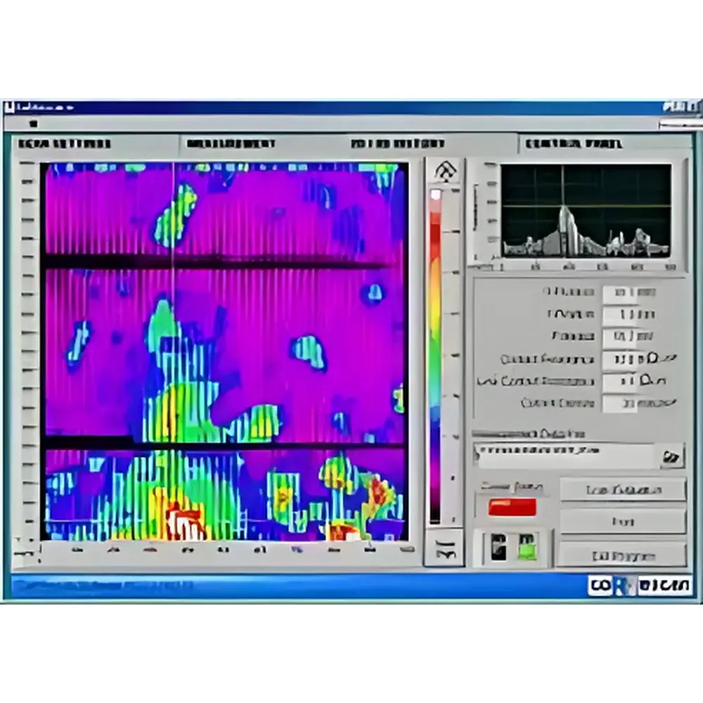
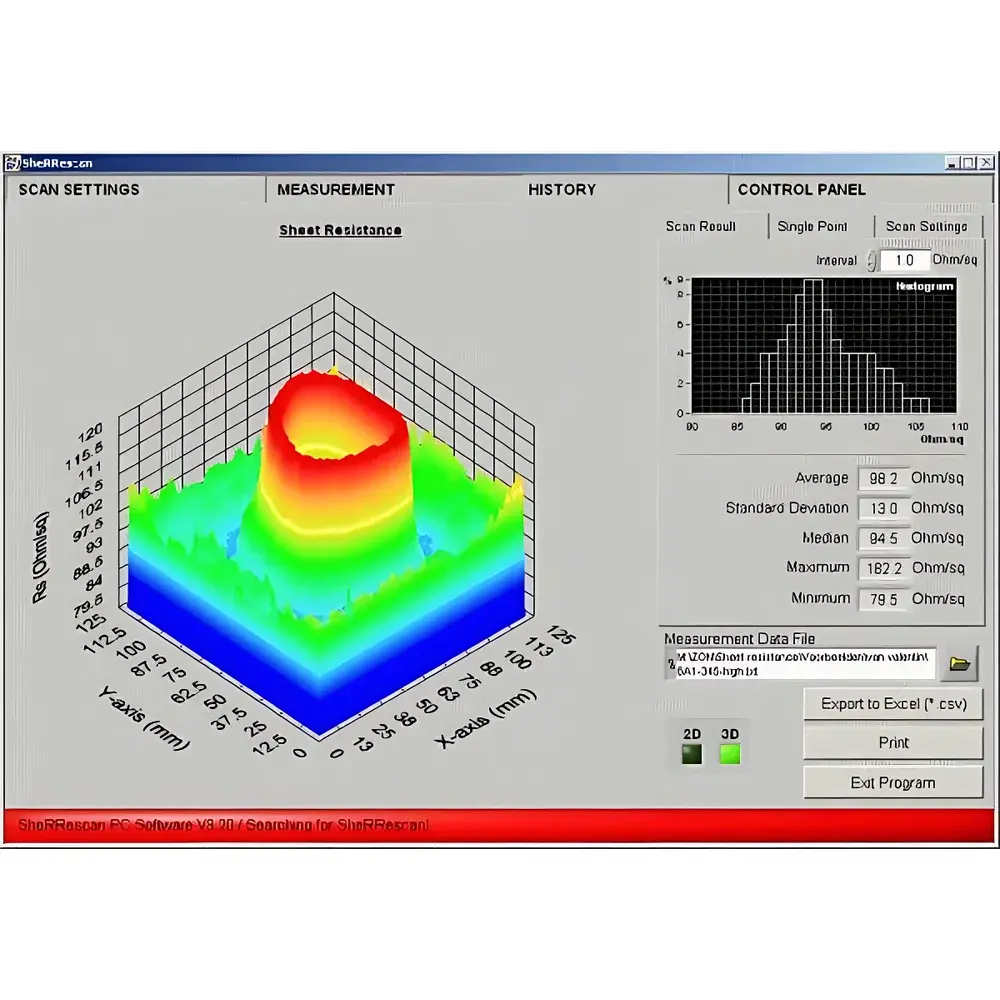
- Simultaneous Rs and Rsh mapping via dual-mode scanning: CoreScan for sheet resistance distribution (μΩ/□ resolution), Sherescan for shunt resistance uniformity (kΩ–MΩ range)
- Integrated VocScan module delivering sub-mV spatial resolution Voc maps under controlled illumination and bias conditions
- LBIC Scan capability with programmable wavelength selection (405 nm to 1064 nm), enabling spectral sensitivity profiling and defect localization across emitter, BSF, and passivation layers
- Motorized XYZ stage with ±0.5 µm repeatability and 150 × 150 mm maximum scan area—compatible with M2, G12, and M10 wafer formats
- Real-time thermal drift compensation and auto-calibration routines compliant with ISO/IEC 17025 traceability requirements
- Modular architecture supporting future upgrades including EL (electroluminescence) and PL (photoluminescence) co-registration
Sample Compatibility & Compliance
The system accommodates bare wafers, textured or planar Si substrates, screen-printed or plated solar cells (including PERC, TOPCon, and heterojunction architectures), and thin-film PV samples up to 2 mm thickness. All measurement protocols adhere to ASTM F3192–22 (Standard Practice for Spatially Resolved Electrical Characterization of Photovoltaic Devices) and IEC 60904-11 (Photovoltaic device calibration standards). Data acquisition and storage meet GLP/GMP audit requirements, with optional 21 CFR Part 11-compliant electronic signatures and audit trail logging available via integrated software configuration.
Software & Data Management
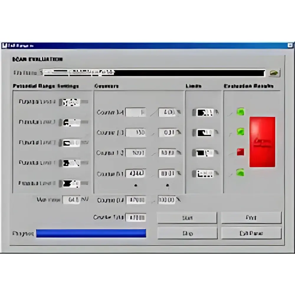
Control and analysis are performed using SunLab’s proprietary ScanSuite v4.2 platform—a Windows-based application featuring intuitive workflow-driven interface, multi-layer overlay visualization (Rs/Rsh/Voc/LBIC superposition), statistical process control (SPC) charting, and automated defect classification using supervised machine learning models trained on >10,000 production-grade PV images. Raw data is exported in HDF5 format with embedded metadata (timestamp, illumination intensity, ambient T/RH, stage position), ensuring full FAIR (Findable, Accessible, Interoperable, Reusable) compliance. Integration with MES/SCADA systems is supported via OPC UA and RESTful API interfaces.
Applications
- Root-cause analysis of firing-related anomalies: over-fired/misfired contacts, phosphosilicate glass (PSG) residue, emitter non-uniformity, and junction leakage
- Process window optimization for screen printing, laser doping, and ALD/PVD passivation steps
- Qualification of new metallization pastes—including Ag/Al composition, glass frit content, and firing profile sensitivity
- Batch-to-batch consistency monitoring for ingot-to-wafer yield correlation studies
- Failure analysis of field-degraded modules via comparative mapping of recovered cells
- Supporting R&D validation of novel cell architectures (e.g., tunnel oxide passivated contacts, selective emitters)
FAQ
What distinguishes CoreScan from conventional four-point probe measurements?
CoreScan delivers full-area, non-contact Rs mapping at >100× higher spatial density than manual probe arrays—and eliminates mechanical pressure artifacts and edge effects inherent in contacting methods.
Can Sherescan detect micro-shunts below 10 kΩ?
Yes; Sherescan achieves effective Rsh detection down to 2 kΩ with SNR > 40 dB under standard 1-scan averaging, validated per IEC 61215-2 MQT 18.1 test conditions.
Is LBIC Scan compatible with bifacial cell evaluation?
Yes—dual-side illumination mode is supported via configurable top/bottom LED arrays and synchronized current sampling, enabling rear-side passivation assessment.
Does the system support automated pass/fail grading against user-defined thresholds?
Yes; ScanSuite includes rule-based binning logic with customizable spatial filters, histogram thresholds, and defect clustering algorithms aligned with internal quality gates.
Are calibration certificates provided with each instrument shipment?
Each unit ships with a factory-issued ISO/IEC 17025-accredited calibration report covering positional accuracy, illumination uniformity, and signal linearity across all operational modes.


