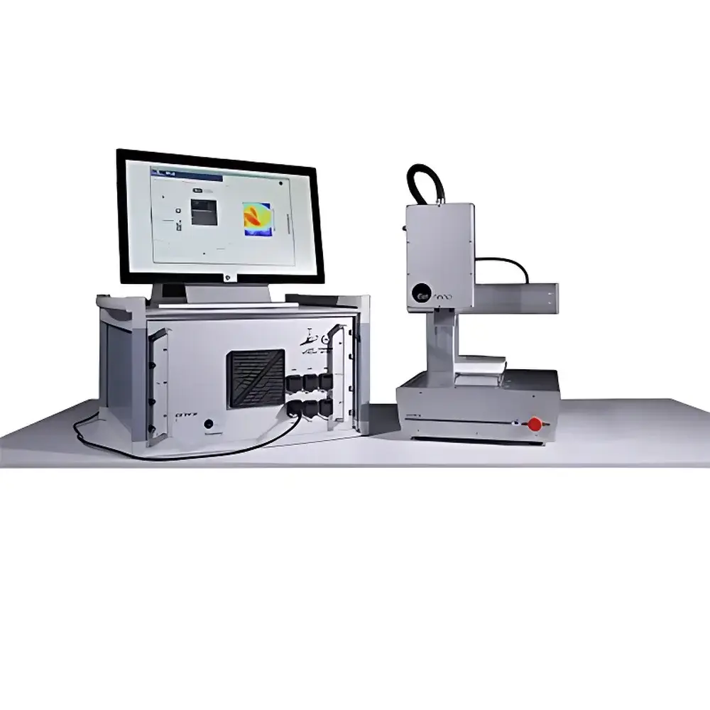
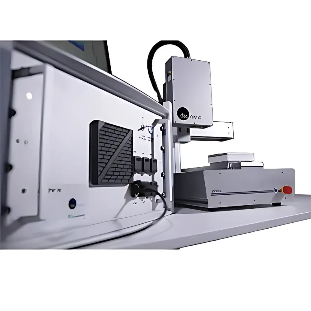
Das-Nano ONYX Terahertz Time-Domain Spectroscopy System for Non-Contact, High-Throughput Electrical Characterization of Graphene and 2D Materials
| Brand | Das-Nano |
|---|---|
| Origin | Spain |
| Model | ONYX |
| Measurement Principle | Pulsed Terahertz Time-Domain Spectroscopy (THz-TDS) |
| Sample Area Range | 10 × 10 mm² to 200 × 200 mm² (customizable up to m² scale) |
| Spatial Resolution | 50 µm |
| Measurement Speed | up to 12 cm²/min |
| Output Parameters | DC conductivity (σ<sub>DC</sub>), carrier concentration (N<sub>s</sub>), drift mobility (μ<sub>drift</sub>), scattering time (τ<sub>sc</sub>), DC resistivity (R<sub>DC</sub>), surface uniformity maps |
| Compliance | Supports GLP/GMP-aligned data audit trails |
Overview
The Das-Nano ONYX is a turnkey terahertz time-domain spectroscopy (THz-TDS) system engineered for non-contact, quantitative, and spatially resolved electrical characterization of graphene, transition metal dichalcogenides (TMDs), conductive polymers, transparent conductive oxides (TCOs), and other two-dimensional (2D) materials. Operating in the 0.1–3 THz spectral range—spanning the far-infrared to sub-millimeter wave regime—the ONYX exploits the unique interaction of pulsed THz radiation with free carriers in semiconducting and semi-metallic thin films. Unlike conventional contact-based methods (e.g., four-point probe or van der Pauw), which yield only pointwise or averaged values and risk mechanical damage or edge effects, the ONYX acquires full-field, pixel-resolved maps of complex conductivity (σ(ω)) by analyzing amplitude and phase shifts of reflected THz transients. Through Fourier transformation of time-domain waveforms and subsequent Drude-model fitting, it extracts fundamental electronic parameters—including DC conductivity (σDC), sheet carrier density (Ns), drift mobility (μdrift), and momentum relaxation time (τsc)—with metrological traceability validated under the European Metrology Programme for Innovation and Research (EMPIR) GRACE project.
Key Features
- Non-contact, non-destructive measurement: Eliminates electrode deposition, lithography, or physical probing—preserving sample integrity across R&D, pilot-line, and production environments.
- Full-area coverage mapping: Scans samples from 10 × 10 mm² (lab-scale coupons) to 200 × 200 mm² (8-inch wafer equivalents); scalable configurations support square-meter substrates for roll-to-roll process monitoring.
- High spatial resolution: 50 µm step resolution enables detection of local heterogeneity, grain boundary effects, and doping gradients unresolvable by macroscopic probes.
- Quantitative parameter extraction: Delivers calibrated σDC, Ns, μdrift, τsc, and RDC without empirical calibration curves—based on first-principles Drude analysis of THz reflectance spectra.
- Sub-second per-pixel acquisition: Achieves throughput up to 12 cm²/min, enabling statistically robust uniformity assessment of large-area CVD graphene, ALD-grown TCOs, or printed PEDOT:PSS films.
- Integrated reflection-mode architecture: Optimized for opaque and semi-transparent substrates (Si, SiO₂/Si, glass, PET, PI), eliminating transmission alignment complexity and supporting backside illumination where needed.
Sample Compatibility & Compliance
The ONYX accommodates a broad spectrum of 2D and thin-film material systems, including monolayer and multilayer graphene (CVD, exfoliated, epitaxial on SiC), reduced graphene oxide (rGO), MoS₂, WS₂, h-BN, NbC, ITO, IZO, ALD-ZnO, TiN, Ag nanowires, GaN quantum dots, and conductive polymer blends (e.g., PEDOT). It requires no vacuum, cryogenic cooling, or ambient control—operating stably under standard laboratory conditions (20–25 °C, 30–60% RH). Data acquisition and processing comply with principles outlined in the EMPIR GRACE Standardization Handbook for Graphene Electrical Measurements (2020), which establishes traceable protocols for THz-TDS-based conductivity mapping. While not certified to ISO/IEC 17025, the system supports audit-ready metadata logging—including instrument configuration, environmental timestamps, raw waveform archives, and version-controlled analysis scripts—facilitating GLP and GMP-aligned workflows where required.
Software & Data Management
ONYX Control Suite is a Windows-based application offering fully automated scan sequencing, real-time waveform visualization, batch-mode parameter fitting, and export-ready reporting. The software implements standardized Drude-model inversion routines compliant with GRACE-recommended fitting constraints (e.g., frequency-dependent screening corrections, substrate permittivity compensation). All raw THz electric field transients are stored in HDF5 format with embedded metadata (sample ID, position, laser power, delay stage status). Processed maps (σDC, Ns, μdrift) export as GeoTIFF or CSV for integration into LIMS or statistical process control (SPC) platforms. Audit trail functionality logs user actions, parameter changes, and software version history—supporting 21 CFR Part 11 readiness when deployed with institutional identity management and electronic signature policies.
Applications
- Graphene manufacturing QC: Rapid uniformity screening of CVD graphene on Cu/Ni foils or transferred films on insulating substrates—identifying wrinkles, tears, polymer residue, and doping inhomogeneity prior to device fabrication.
- Transparent conductor development: Quantitative comparison of sheet resistance and carrier mobility across ITO, AZO, FTO, and emerging alternatives (e.g., AgNW networks, carbon nanotube meshes) at production-relevant scales.
- 2D semiconductor process optimization: Correlating ALD/MBE growth parameters (temperature, precursor dose, annealing) with spatially resolved μdrift and Ns in MoS₂ or WSe₂ channels.
- Photovoltaic interlayer validation: Mapping lateral conductivity of hole-transport layers (e.g., PEDOT:PSS, NiOx) beneath perovskite absorbers to diagnose shunt path formation.
- Standards reference metrology: Serving as a primary method in inter-laboratory comparisons coordinated by NMIs (e.g., NPL, PTB, CENAM) for validating contact-based measurements against non-contact benchmarks.
FAQ
How does ONYX differ from four-point probe or van der Pauw measurements?
ONYX provides full-field, non-contact conductivity maps at 50 µm resolution, whereas contact methods deliver single-point or area-averaged values and introduce artifacts from probe placement, contact resistance, and edge effects.
Can ONYX measure on flexible or curved substrates?
Yes—its reflection geometry and motorized Z-axis focus compensation accommodate substrates with up to ±2 mm surface topography, including PET, PI, and thin metal foils.
Is calibration required before each measurement?
No routine recalibration is needed; the system uses internal reference measurements (gold mirror, air baseline) to maintain amplitude and phase stability over multi-hour sessions.
Does ONYX support thickness-independent carrier density extraction?
For monolayer or few-layer 2D materials where thickness is ill-defined, ONYX reports sheet carrier density (Ns, in cm⁻²); for thicker semiconductors (>10 nm), volumetric N (cm⁻³) can be derived if thickness is known independently.
What level of expertise is required to operate ONYX?
Operators require basic familiarity with thin-film metrology concepts; full training—including GRACE-compliant measurement protocols—is provided during installation and documented in the operational manual.
")


