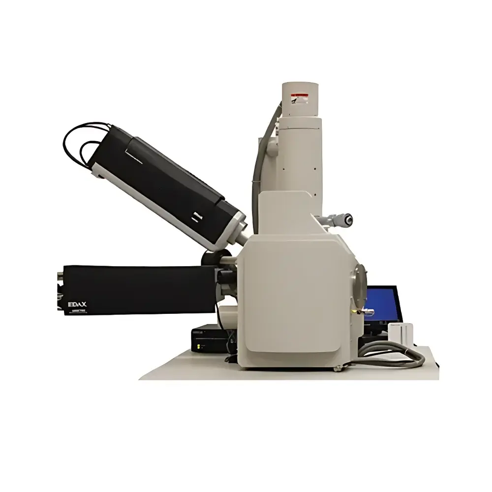
EDAX TEAM™ Pegasus EDS-EBSD Integrated Microanalysis System
| Brand | EDAX |
|---|---|
| Origin | USA |
| Model | TEAM™ Pegasus (EDS-EBSD) |
| Detector Type | Integrated Energy Dispersive Spectrometer (EDS) and Electron Backscatter Diffraction (EBSD) System |
| EDS Detector Options | Octane Elect or Octane Elite Silicon Drift Detector (SDD) |
| EBSD Camera Options | Velocity™ Super, Orion™, Hikari Super, DigiView |
| Energy Resolution | <127 eV at Mn Kα (typical for Octane Elite SDD) |
| Peak-to-Background Ratio | >3,500:1 (at 5 kcps, Mn Kα) |
| Maximum Input Count Rate | Up to 2.5 Mcps (Octane Elite) |
| Active Detector Area | 100 mm² (Octane Elite) |
| EBSD Camera Frame Rate | Up to 3,000 fps (Velocity™ Super, full-frame) |
| Spatial Resolution (EBSD) | ≤0.05° angular resolution (confidence index ≥0.1) |
| Software Platform | TEAM™ v5.x with real-time indexing, EXpert ID, and automated background subtraction |
Overview
The EDAX TEAM™ Pegasus EDS-EBSD Integrated Microanalysis System is a high-performance, synchronized microstructural and compositional characterization platform designed for integration with scanning electron microscopes (SEM) and dual-beam FIB-SEM systems. It combines energy-dispersive X-ray spectroscopy (EDS) and electron backscatter diffraction (EBSD) into a single, co-registered acquisition workflow—enabling simultaneous, pixel-matched collection of elemental composition (via characteristic X-ray emission) and crystallographic orientation (via Kikuchi band pattern analysis). This correlation is foundational for advanced materials science investigations, including phase mapping, grain boundary characterization, texture analysis, strain evaluation, and failure mechanism studies. The system operates on the principle of electron–solid interactions: incident electrons generate both characteristic X-rays (for EDS) and backscattered electrons forming diffraction patterns (for EBSD), both detected in real time without stage repositioning or signal crosstalk. Its architecture is engineered for precision, stability, and reproducibility under variable beam conditions (5–30 kV), making it suitable for routine quality control as well as cutting-edge R&D in metallurgy, geoscience, semiconductor development, and additive manufacturing.
Key Features
- Synchronized EDS-EBSD data acquisition with sub-micron spatial registration and temporal alignment—ensuring direct pixel-by-pixel correlation between chemistry and crystallography.
- Modular detector configuration: choice of Octane Elect or Octane Elite silicon drift detectors (SDDs), delivering high count-rate capability (up to 2.5 Mcps), excellent energy resolution (3,500:1).
- Flexible EBSD camera selection—including Velocity™ Super (CMOS-based, up to 3,000 fps full-frame), Orion™ (low-noise, high-fidelity pattern acquisition), Hikari Super (optimized sensitivity-speed balance), and DigiView (high-resolution static analysis)—to match application-specific throughput and fidelity requirements.
- TEAM™ v5.x software with EXpert ID: fully automated, real-time spectrum identification and phase matching using integrated reference libraries (ICDD PDF-4+, EDAX Phase Library); supports multi-phase quantification and ZAF/φ(ρz) matrix corrections.
- Intelligent auto-optimization suite: automatic EBSD camera focus, working distance calibration, pattern center determination, and dynamic background subtraction—reducing operator dependency and improving inter-laboratory reproducibility.
- Robust hardware synchronization: proprietary FPGA-based timing control ensures nanosecond-level coordination between EDS pulse processing and EBSD frame capture, eliminating latency-induced misregistration.
Sample Compatibility & Compliance
The TEAM™ Pegasus system is compatible with conductive and semi-conductive bulk samples, polished cross-sections, thin foils, and coated particulates—provided standard SEM preparation protocols are followed (e.g., carbon or chromium coating for non-conductive specimens). It complies with ISO/IEC 17025 requirements for testing laboratories when used within validated workflows. Data acquisition and reporting support GLP/GMP traceability through optional audit trail logging, electronic signatures, and 21 CFR Part 11–compliant software modules. All spectral and orientation data adhere to the ASTM E1508 (EDS quantitative analysis) and ASTM E2627 (EBSD pattern indexing) standards. Exportable results conform to the HDF5-based EMsoft and NIST MSF file formats for third-party interoperability.
Software & Data Management
TEAM™ v5.x provides an intuitive, tab-driven interface with integrated project management, allowing users to define acquisition templates, batch-process maps, and apply post-acquisition filters (e.g., confidence index masking, phase thresholding, grain dilation). Raw EDS spectra and EBSD patterns are stored with full metadata (beam parameters, detector geometry, calibration timestamps). The software supports scripting via Python API for custom quantification routines and machine-learning–assisted phase classification. Data export includes CSV, TIFF, ODF, and Crystallographic Information File (CIF) formats. Cloud-synced project archives and role-based access control enable collaborative analysis across distributed teams while maintaining version integrity and chain-of-custody records.
Applications
- Phase identification and distribution mapping in multiphase alloys (e.g., Ni-based superalloys, Ti-6Al-4V, Al-Si castings).
- Grain boundary engineering: Σ3–Σ29 CSL boundary statistics, twin detection, and recrystallization kinetics in cold-rolled steels and aluminum foils.
- Residual stress estimation via high-resolution EBSD (HR-EBSD) combined with EDS-derived lattice parameter shifts.
- Geological provenance analysis: simultaneous mineral identification (EDS) and crystallographic orientation (EBSD) in zircon, quartz, and olivine aggregates.
- Failure analysis: correlating intergranular corrosion sites (elemental segregation) with local misorientation gradients and boundary character.
- Thin-film and heterostructure characterization in semiconductor devices, including epitaxial layer registry and defect density mapping.
FAQ
Can TEAM™ Pegasus operate independently of an SEM?
No—it is a dedicated add-on system requiring integration with a field-emission SEM or FIB-SEM equipped with appropriate EDS and EBSD ports, stage control, and digital I/O interfaces.
What level of training is required to achieve reliable EBSD indexing?
Basic operation requires minimal training due to intelligent auto-setup; however, advanced interpretation (e.g., HR-EBSD, pattern distortion correction) benefits from foundational knowledge in crystallography and diffraction physics.
Is offline reprocessing supported for previously acquired EBSD maps?
Yes—TEAM™ v5.x allows full recalibration, re-indexing, and confidence-based filtering of archived .ebsp files using updated reference patterns or refined indexing parameters.
How does the system handle beam-sensitive or insulating samples?
Low-dose acquisition modes, variable dwell time per pixel, and charge-compensation-compatible detector geometries minimize damage and charging artifacts—particularly when paired with low-kV imaging and beam deceleration.
Are custom reference databases supported for proprietary phases?
Yes—users may import and validate custom crystal structure files (.cif) and integrate them into EXpert ID’s searchable library with user-defined confidence thresholds and exclusion rules.


