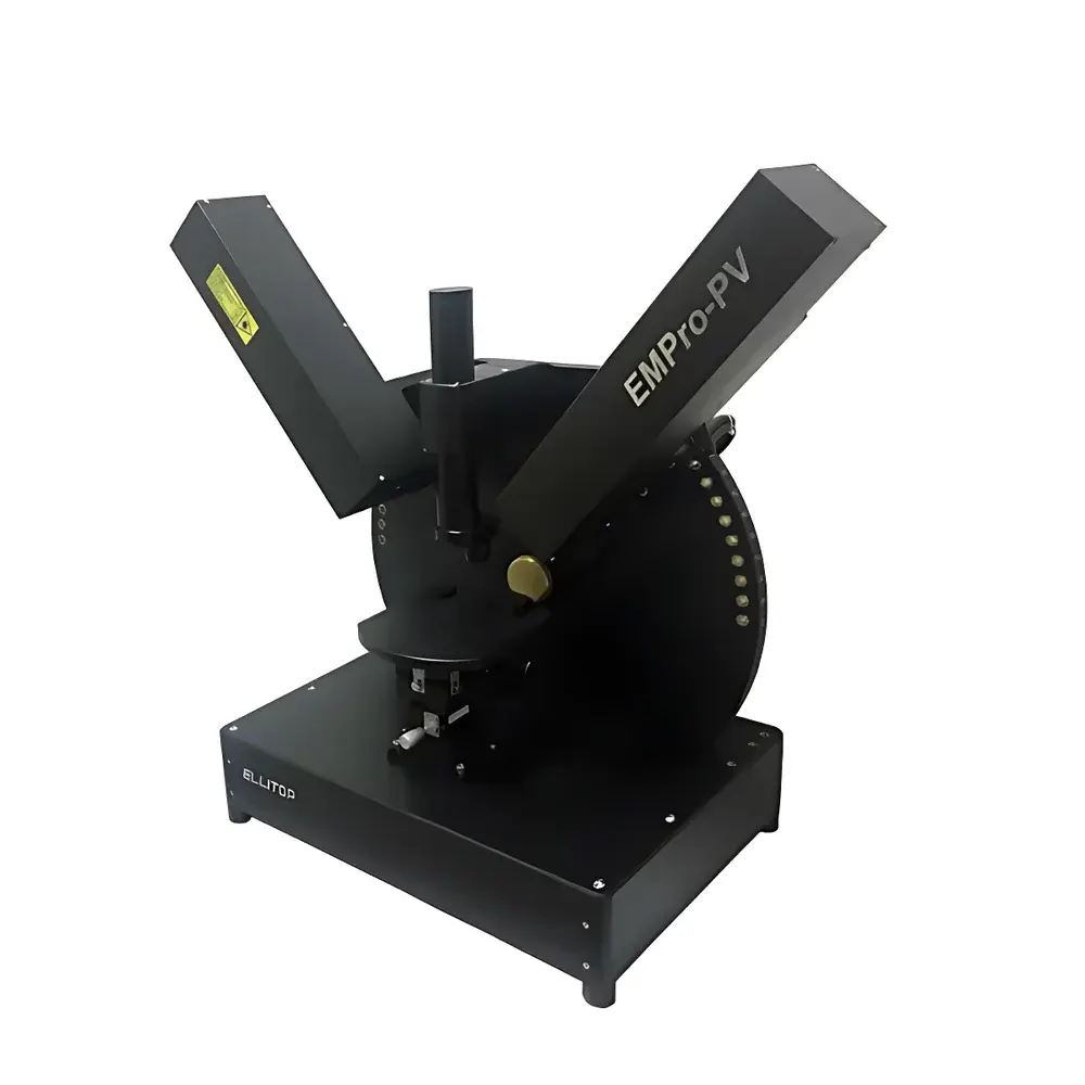
ELLITOP EMPro-PV Photovoltaic-Specific Laser Ellipsometer
| Brand | ELLITOP |
|---|---|
| Origin | Beijing, China |
| Model | EMPro-PV |
| Spot Size | <1 mm |
| Incident Angle Range | 40°–90° (manually adjustable in 5° increments) |
| Single-Measurement Time | 0.6 s (typical) |
Overview
The ELLITOP EMPro-PV is a high-precision, multi-angle laser ellipsometer engineered specifically for photovoltaic (PV) R&D laboratories and inline quality control environments. It operates on the principle of spectroscopic ellipsometry—specifically, rotating-compensator (RC) ellipsometry—at a fixed wavelength of 632.8 nm (He–Ne laser). This configuration enables non-destructive, contactless characterization of optical constants (refractive index *n* and extinction coefficient *k*) and geometric parameters—including thickness, roughness, and interfacial grading—of thin-film coatings on both planar and textured silicon substrates. The instrument is optimized for measuring anti-reflection (AR) coatings on mono- and multicrystalline silicon solar cells, where surface texturing introduces strong light scattering and low specular reflectance. Its RC architecture ensures full Δ coverage from 0° to 360°, eliminating measurement singularities near Brewster’s angle or at near-normal incidence—critical for robust metrology on industrially relevant PV surfaces.
Key Features
- Rotating-compensator ellipsometry architecture with full 0°–360° delta measurement range—no blind zones, even at critical angles (e.g., 0° or 180°)
- Dedicated PV sample stage integrating mono- and multicrystalline silicon compatibility via mechanical interchange—switching completed in under 10 seconds without realignment
- Sub-millimeter laser spot (<1 mm diameter) enabling localized metrology on individual pyramids or grain boundaries of textured wafers
- Manually adjustable incident angle from 40° to 90° in precise 5° increments—supports sensitivity optimization across film stack configurations
- Video-assisted optical auto-alignment system with telecentric microscope optics for rapid, micron-level sample positioning and azimuthal orientation
- Low-noise photodetection electronics combined with proprietary signal enhancement algorithms—designed to recover weak specular signals from highly scattering, low-reflectance PV surfaces
- Integrated mechanical and optical design minimizing thermal drift and vibration coupling—optimized for factory-floor deployment near production lines
Sample Compatibility & Compliance
The EMPro-PV accommodates standard 156 mm × 156 mm (M2), 166 mm × 166 mm (G12), and 182 mm × 182 mm (M10) silicon wafers, including those with random pyramid textures (height: 1–5 µm) or planar passivation layers (SiNx, AlOx, SiO2, TiO2). It supports single-layer and multilayer stack analysis—such as SiNx/SiO2 bilayers or graded SiNx films—using physically constrained optical models. The system complies with ISO/IEC 17025 traceability requirements for calibration of optical thickness standards. Measurement workflows align with ASTM E1939 (Standard Guide for Use of Spectroscopic Ellipsometry in Semiconductor Manufacturing) and support GLP/GMP documentation protocols, including user role-based access control (administrator/operator modes), audit-trail logging, and exportable measurement reports compliant with internal QC templates.
Software & Data Management
The instrument is controlled via ELLITOP’s proprietary EMPro software suite, featuring a one-click multithreaded interface optimized for high-throughput operation. The software includes an extensive library of optical dispersion models (Cauchy, Tauc-Lorentz, Cody-Lorentz) and pre-characterized material databases (e.g., crystalline Si, amorphous Si, SiNx stoichiometries, ITO) for rapid model initialization. All fitting routines employ Levenberg–Marquardt nonlinear least-squares minimization with confidence interval estimation. Raw Ψ/Δ data, fit residuals, and covariance matrices are stored in HDF5 format. Export options include CSV, XML, and PDF reports—with configurable metadata fields (operator ID, timestamp, lot number, recipe name) to support MES integration. Software validation documentation is available upon request for FDA 21 CFR Part 11–aligned environments.
Applications
- Thickness and optical constant monitoring of SiNx anti-reflection coatings on industrial PERC, TOPCon, and HJT solar cells
- In-line process verification of plasma-enhanced chemical vapor deposition (PECVD) and atomic layer deposition (ALD) steps
- Characterization of interfacial oxide layers at Si/SiNx and Si/AlOx heterojunctions
- Quantification of surface texturing effects on effective optical thickness and gradient layer formation
- Reference measurements for calibrating inline reflectometers and spectrophotometers used in PV manufacturing
- R&D of novel passivation stacks, including SiOx/a-Si:H bilayers and nanocrystalline silicon emitters
FAQ
What is the minimum measurable thickness for SiNx on textured silicon?
For typical pyramid-textured c-Si with RMS roughness ~0.5–1 µm, the practical lower limit is ~20 nm with ±0.3 nm repeatability (3σ, n=10) under standard calibration conditions.
Can the EMPro-PV measure beyond 632.8 nm?
No—the system is configured exclusively for He–Ne laser operation at 632.8 nm. For spectral ellipsometry, ELLITOP offers the EMPro-S series.
Is remote diagnostics supported?
Yes—via secure TLS-encrypted VNC session with prior authorization; all diagnostic logs comply with ISO/IEC 27001 data handling guidelines.
How often does the system require recalibration?
Annual calibration is recommended per ISO/IEC 17025; optional quarterly verification kits (NIST-traceable SiO2/Si reference wafers) are available.
Does the software support custom scripting for automated batch analysis?
Yes—Python API access is provided under NDA for integration into LabVIEW, MATLAB, or Python-based SPC platforms.