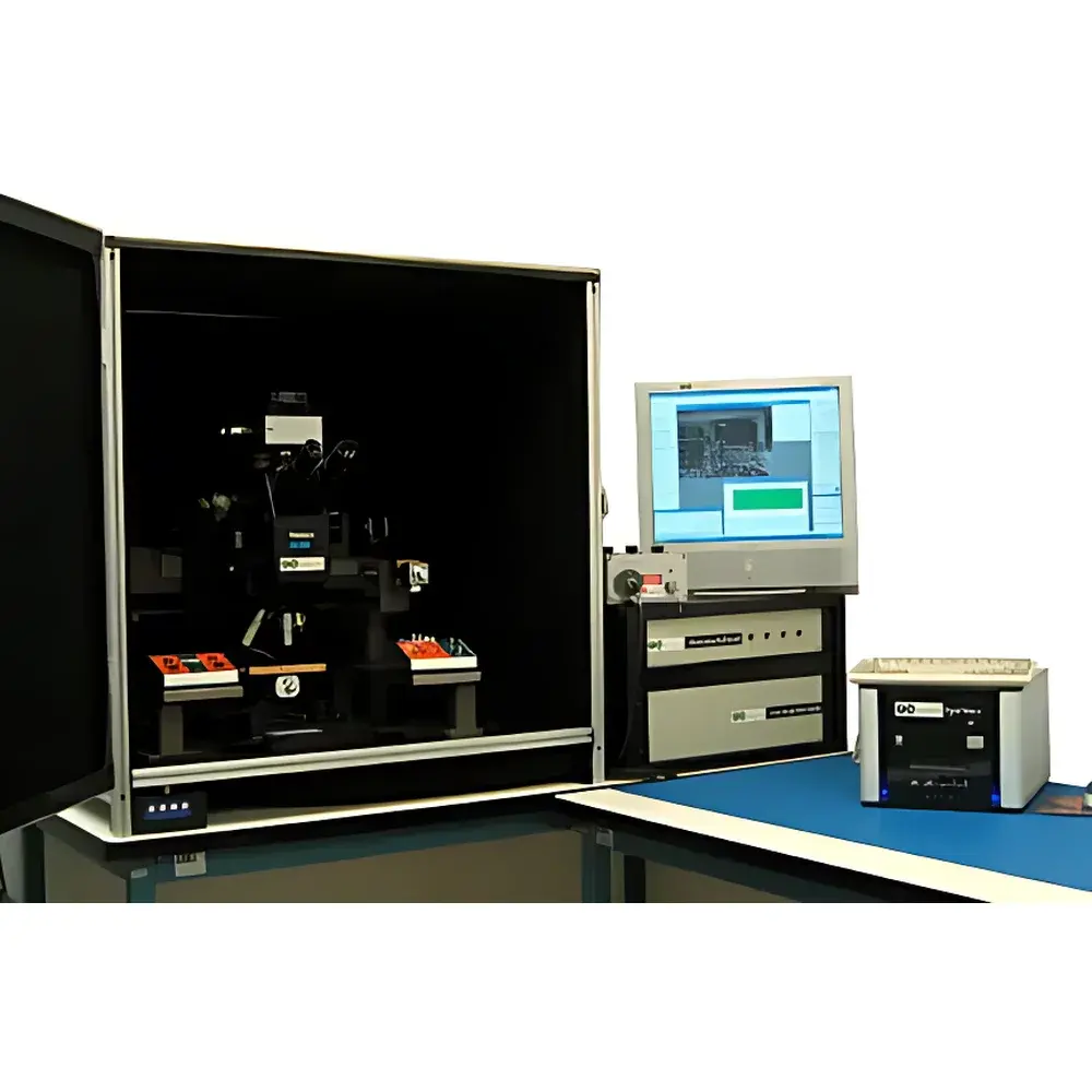
FAI Crystal Vision Photoemission Microscope
| Origin | USA |
|---|---|
| Manufacturer Type | Authorized Distributor |
| Origin Category | Imported |
| Model | FAI Crystal Vision Photoemission Microscope |
| Pricing | Available Upon Request |
Overview
The FAI Crystal Vision Photoemission Microscope is a high-sensitivity, multi-modal failure analysis instrument engineered for non-invasive localization of active defects in semiconductor devices and integrated circuits. It operates on the principle of detecting ultra-low-intensity photon emissions (photons per second in the range of 10⁰–10³) generated by localized energy dissipation mechanisms—including carrier recombination at defect sites, hot-carrier injection, gate oxide breakdown, latch-up, and Joule heating. Unlike conventional optical microscopy, this system integrates time-resolved, wavelength-resolved, and stimulus-synchronized detection to distinguish between photonic (EMMI), thermal (FMI/SLC), and laser-induced fault signatures—enabling precise spatial correlation of electrical failure with physical location at sub-micron resolution.
Key Features
- Modular detector architecture supporting simultaneous or sequential integration of up to four independent detectors: back-illuminated CCD, InGaAs, VisGaAs, and optional UV-enhanced sensors—each cooled via solid-state thermoelectric (TEC) to ≤ −40 °C without cryogenic liquids.
- CCD detector: 1280 × 1024 pixels, spectral response 365–1190 nm, dark current <0.002 e⁻/s/pixel, read noise <7 e⁻ RMS, integration time adjustable from 32 ms to 2 hours.
- InGaAs detector: 320 × 240 pixels, 30 × 30 µm pixel pitch, spectral range 900–1750 nm, peak quantum efficiency 80–85%, NEI <1 × 10¹⁰ ph/cm²/s, integration time from 1 µs to 60 minutes.
- VisGaAs detector: Unified visible-to-shortwave-infrared coverage (500–1800 nm), eliminating need for detector swapping; TEC-cooled to ≤ −40 °C.
- SIFT dual-wavelength laser scanning head: Integrated 654 nm (visible) and 1428 nm (SWIR) diode lasers with galvo-based raster scanning; constant-current feedback loop ensures stable bias during stimulation and prevents overvoltage-induced secondary damage.
- FMI (Fluorescence Microthermal Imaging): Thermal resolution ≤ 0.001 K at ambient temperature; no liquid crystal media required.
- SLC (Stabilized Liquid Crystal) thermal imaging: Resolution ≤ 0.01 K; calibrated for quantitative junction temperature mapping.
- Moire-based backside thermal mapping: Enables non-contact, full-wafer-scale thermal anomaly detection through silicon substrate using interference fringe analysis.
Sample Compatibility & Compliance
The Crystal Vision system accommodates packaged ICs (QFP, BGA, CSP), bare die on probe stations, and wafer-level samples (up to 300 mm). Its optical path supports both front-side and backside illumination/detection configurations, compatible with standard microscope stages and vacuum-compatible sample holders. All hardware and software modules comply with ISO/IEC 17025 traceability requirements for metrological validation. Data acquisition workflows support audit-ready logging per FDA 21 CFR Part 11 and GLP/GMP documentation standards—including user authentication, electronic signatures, and immutable timestamped event records.
Software & Data Management
Control and analysis are managed via FAI’s proprietary VisionSuite™ platform—a Windows-based application with modular plug-ins for EMMI, SIFT, FMI, SLC, and Moire imaging. The software enables real-time overlay of photonic and thermal maps, cross-correlation of laser-stimulated signal transients with electrical I/V waveforms (via external oscilloscope synchronization), and automated defect centroid calculation with sub-pixel interpolation. Raw data is stored in HDF5 format with embedded metadata (wavelength, integration time, bias conditions, detector gain, laser power), ensuring long-term reproducibility and third-party interoperability. Export options include TIFF, CSV, and MATLAB-compatible binaries for statistical process control (SPC) integration.
Applications
- Root-cause analysis of parametric failures in advanced nodes (≤ 5 nm FinFET, GAA, and 3D NAND).
- Identification of gate oxide pinholes, ESD damage paths, and electromigration voids.
- Verification of design-for-test (DFT) structures and scan chain integrity under functional stress.
- Thermal profiling of power devices (SiC MOSFETs, GaN HEMTs) during dynamic switching.
- Qualification of wafer-level reliability tests (HTOL, ESD, TC) via spatially resolved emission mapping.
- Failure mode validation for automotive AEC-Q100 Grade 0/1 components and aerospace radiation-hardened ICs.
FAQ
What is the minimum detectable photon flux for the CCD detector under −40 °C cooling?
At full cooling and optimal gain settings, the system achieves a single-photon detection limit of ≈ 100 photons/pixel/sec with 1-second integration—validated against NIST-traceable calibrated light sources.
Can the SIFT laser scanning be synchronized with external electrical stimulus generators?
Yes—VisionSuite supports TTL and LVDS trigger inputs for precise alignment of laser pulses with voltage/current ramps, square-wave stimuli, or arbitrary waveform generator (AWG) outputs.
Is the VisGaAs detector suitable for detecting emissions from silicon carbide (SiC) devices?
Yes—the extended 500–1800 nm spectral range captures both band-edge luminescence (~390 nm for SiC) and defect-related mid-IR emissions up to 1700 nm, enabling comprehensive characterization without detector changeover.
Does the system support automated defect navigation across multiple dies on a full wafer?
Via integration with third-party wafer probers (e.g., Cascade Summit, FormFactor), the system supports coordinate-based stage movement and recipe-driven batch analysis with auto-focus and exposure optimization per site.
How is thermal calibration performed for FMI and SLC modes?
Factory calibration uses blackbody reference sources at three temperatures (25 °C, 50 °C, 85 °C); field recalibration is supported via built-in Peltier-controlled reference targets traceable to ITS-90.


