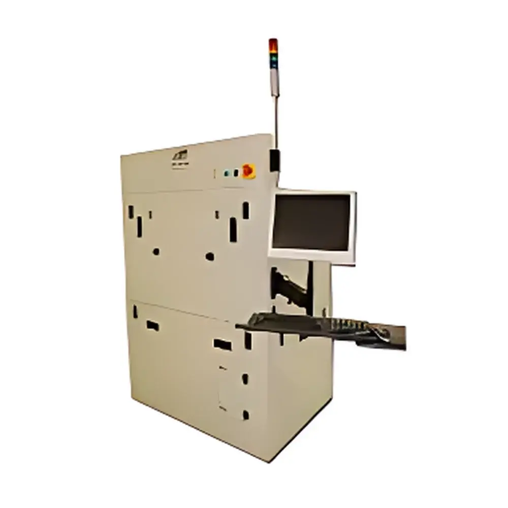
FSM FSM-413 EC Non-Contact Wafer Thickness & Depth Metrology System
| Brand | FSM |
|---|---|
| Origin | USA |
| Model | FSM-413 EC |
| Measurement Principle | Infrared (IR) Interferometric EchoProbe™ Technology |
| Substrate Compatibility | Si, GaAs, InP, SiC, Sapphire, Quartz, Glass, Polymers |
| Configurations | Single-Probe (substrate thickness only) / Dual-Probe (total thickness + topography) |
| Optional Modules | Trench/Through-Silicon Via (TSV) Depth, Film Thickness, Bump Height, Surface Roughness (Rq/Ra), Sidewall Angle |
| Compliance | Designed for ISO 9001-certified semiconductor fabrication environments |
Overview
The FSM FSM-413 EC is a precision non-contact metrology platform engineered for in-line and laboratory-based thickness and depth characterization of semiconductor wafers, compound semiconductor substrates, and advanced packaging structures. It employs proprietary EchoProbe™ infrared interferometry — a coherent optical technique operating in the near-infrared spectral range (typically 1.0–1.7 µm) — to resolve optical path differences between multiple reflective interfaces within transparent or semi-transparent materials. Unlike contact profilometers or capacitance-based systems, the FSM-413 EC delivers sub-nanometer resolution in thickness differential measurements without mechanical loading, surface contamination, or risk of wafer breakage. Its core capability lies in resolving discrete echo signals from air/substrate, substrate/adhesive, adhesive/carrier, and carrier/air boundaries — enabling unambiguous separation of substrate thickness, tape-induced offset, bonding layer thickness, and topographical features such as MEMS actuators, redistribution layers (RDL), or copper pillars. The system is calibrated traceably to NIST standards and validated per SEMI MF-1530 for wafer thickness uniformity (TTV) reporting.
Key Features
- Single-probe configuration optimized for high-accuracy substrate thickness measurement on IR-transparent wafers — including Si (up to 1000 µm), GaAs, InP, SiC, sapphire, fused silica, and select polymer films.
- Dual-probe architecture enables simultaneous front-surface and back-surface interrogation, supporting total thickness measurement (TT) and calculation of structural parameters such as bond layer thickness, adhesive compression, and carrier-induced bow compensation.
- Sub-100 µm thin wafer capability: Validated performance on mechanically ground, chemically thinned, and plasma-etched wafers down to 20 µm substrate thickness with ≤0.2 µm repeatability (3σ) under controlled environmental conditions.
- Pattern-aware measurement: Robust signal acquisition across structured surfaces — including photolithographically defined trenches, etched vias, metal bumps, dielectric stacks, and tape-mounted wafers on blue film or UV-curable carriers.
- Modular expansion support: Field-upgradable options include high-aspect-ratio trench depth profiling (up to 100:1 AR), conformal film thickness mapping (SiO₂, SiNₓ, polyimide), solder bump height quantification, and sidewall angle estimation via multi-angle echo deconvolution.
Sample Compatibility & Compliance
The FSM-413 EC accommodates standard wafer formats from 100 mm to 300 mm diameter, including edge-excluded and notch-aligned configurations. It accepts wafers mounted on frame-mounted dicing tape, temporary bonding carriers (e.g., glass or silicon handles), and vacuum chucks with customizable flatness compensation algorithms. Material compatibility extends beyond elemental semiconductors to III–V compounds, wide-bandgap oxides, and heterogeneous integration stacks used in RF, power, and photonics applications. The system conforms to SEMI E10 (Definition of Terms Relating to Semiconductor Manufacturing Equipment), SEMI E11 (Equipment Communication Standard), and supports integration into factory automation via SECS/GEM protocol. Data output complies with ASTM E2658 (Standard Practice for Determining Thickness of Transparent Films Using Interferometry) and is compatible with SPC charting tools compliant with ISO/IEC 17025 requirements.
Software & Data Management
The FSM Control Suite v5.x provides intuitive workflow-driven operation, including automated recipe-based measurement sequencing, spatial grid definition (radial, spiral, or user-defined), and real-time thickness contour mapping. All raw interferograms and processed results are stored in vendor-neutral HDF5 format with embedded metadata (timestamp, operator ID, environmental sensor logs, calibration epoch). Audit trails meet FDA 21 CFR Part 11 requirements through role-based access control, electronic signatures, and immutable log history. Export modules support CSV, XML, and industry-standard GDSII-compatible thickness map files for integration with yield management platforms (e.g., PDF Solutions, KLA Yield Explorer).
Applications
- Post-grind thickness control and TTV assessment for 3D IC and advanced packaging processes.
- TSV depth and bottom-top profile characterization in through-silicon via fabrication.
- MEMS device metrology: cavity depth, membrane thickness, comb-drive gap verification, and release etch endpoint confirmation.
- LED manufacturing: sapphire and SiC substrate thickness uniformity, epitaxial layer stack monitoring (when combined with optional spectral reflectance module), and wafer bow compensation during epitaxy tool qualification.
- Fan-out wafer-level packaging (FOWLP): mold compound thickness, RDL line height, and die attach void detection via differential echo amplitude analysis.
- Compound semiconductor foundry QC: InP-based photonic integrated circuit (PIC) substrate thickness, GaN-on-Si HEMT buffer layer evaluation, and AlN piezoelectric film thickness mapping.
FAQ
What materials can the FSM-413 EC measure?
It measures IR-transparent substrates including silicon, gallium arsenide, indium phosphide, silicon carbide, sapphire, quartz, glass, and selected polymers. Opaque or highly scattering materials (e.g., thick metal films, carbon-doped layers) require dual-probe or complementary techniques.
Does it require vacuum or nitrogen purge for operation?
No — the system operates stably in ambient cleanroom environments (Class 100–1000); optional purge kits are available for moisture-sensitive applications involving hygroscopic adhesives or low-k dielectrics.
Can it measure bonded wafers with intermediate layers?
Yes — the EchoProbe™ algorithm resolves up to four distinct echo interfaces, enabling independent quantification of substrate, bonding layer (e.g., oxide, polymer, or metal), and carrier thickness.
Is calibration traceable to national standards?
Yes — factory calibration uses NIST-traceable step-height standards and certified reference wafers; on-site recalibration kits include Si/SiO₂ thickness standards certified per ISO/IEC 17025.
How is measurement uncertainty reported?
Uncertainty budgets follow GUM (Guide to the Expression of Uncertainty in Measurement) principles and include contributions from laser wavelength stability, detector noise floor, environmental drift (temperature/humidity), and stage positioning repeatability — all documented in the system’s Certificate of Conformance.


