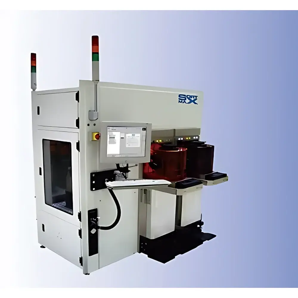
Genmark Sort-Max Wafer Sorter
| Brand | Genmark |
|---|---|
| Origin | USA |
| Manufacturer Type | Authorized Distributor |
| Product Origin | Imported |
| Model | Sort-Max Wafer Sorter |
| Pricing | Available Upon Request |
Overview
The Genmark Sort-Max Wafer Sorter is an industrial-grade, high-precision automated handling system engineered for front-end semiconductor fabrication environments. It operates on a closed-loop motion control architecture integrated with vacuum-based end-effectors and non-contact optical alignment sensors to ensure sub-millimeter placement accuracy and zero-scratch wafer transport. Designed specifically for 100 mm (4″) to 300 mm (12″) silicon wafers and photomasks, the Sort-Max supports full-wafer batch processing in cleanroom-compatible Class 100 (ISO Class 5) or better environments. Its core functionality centers on deterministic wafer routing—enabling precise lot segregation, FOUP (Front Opening Unified Pod) balancing, ID verification via integrated barcode/RFID readers, and real-time status logging—all synchronized to factory automation protocols including SECS/GEM and HSMS.
Key Features
- High-throughput sorting: Achieves cycle times under 8 seconds per wafer at 300 mm, scalable across mixed-diameter lots without mechanical reconfiguration.
- Self-calibrating kinematic platform: Automatically compensates for thermal drift and mechanical wear using embedded encoder feedback and reference fiducial mapping.
- Cleanroom-optimized design: All internal transport paths are constructed from low-outgassing stainless steel and electrostatic-dissipative polymers; particle generation < 0.1 particles ≥ 0.5 µm per cubic foot per minute (per SEMI S2-0216).
- Modular configurability: Supports optional integration of inline macro/micro defect inspection modules, edge-profile scanners, and metrology-triggered sort logic based on pre-loaded yield maps.
- FOUP-centric workflow management: Native support for standard 25-wafer FOUPs (SEMI E47.1 compliant), including pod weight verification, lid-seal integrity check, and dynamic load balancing across multiple input/output ports.
Sample Compatibility & Compliance
The Sort-Max accommodates bare and patterned silicon wafers, SOI substrates, compound semiconductors (GaAs, SiC), and quartz photomasks ranging from 100 mm to 300 mm in diameter. Edge exclusion is configurable down to 1.5 mm. The system complies with SEMI E11 (Equipment Communications Standard), SEMI E30 (GEM), SEMI E47.1 (FOUP specifications), and ISO 14644-1 Class 5 cleanroom requirements. Electrical safety conforms to UL 61010-1 and IEC 61000-6-2/6-4 for industrial electromagnetic compatibility.
Software & Data Management
Controlled by Genmark’s proprietary SortWare™ v4.x platform, the Sort-Max provides audit-trail-enabled operation logs compliant with FDA 21 CFR Part 11 and ISO 9001 traceability requirements. All sort decisions, sensor readings, FOUP metadata, and operator actions are timestamped, digitally signed, and exportable in CSV or XML formats. The software supports recipe-driven sorting rules—including yield-bin mapping, process-layer filtering, and metrology-linked disposition—and integrates natively with MES systems via standard TCP/IP-based APIs. Optional validation packages include IQ/OQ documentation aligned with GMP/GLP laboratory practices.
Applications
- Front-end fab wafer sort prior to lithography or etch steps
- Post-process yield segregation in advanced packaging lines (e.g., fan-out wafer-level packaging)
- Research lab wafer triage for materials qualification and failure analysis sample preparation
- Foundry multi-customer lot consolidation and de-consolidation with traceable chain-of-custody
- Mask shop inventory management and reticle tracking with dual-ID (mask ID + wafer ID) correlation
FAQ
Does the Sort-Max support 450 mm wafers?
No—the current mechanical and control architecture is certified for 100–300 mm substrates only; 450 mm capability is not available in production configuration.
Can it interface with third-party metrology tools?
Yes—via standard SECS/GEM messaging or custom RESTful API adapters, enabling bidirectional data exchange with CD-SEM, overlay metrology, and film-thickness measurement systems.
Is remote diagnostics supported?
Yes—Genmark offers optional Secure Remote Access (SRA) module with TLS 1.2 encryption and role-based access control for Tier-2 technical support and firmware updates.
What maintenance intervals are recommended?
Preventive maintenance is scheduled every 2,000 operational hours or annually, whichever occurs first; consumables include vacuum filters, encoder calibration targets, and FOUP interface gaskets.
Does it meet ESD protection standards for device-grade handling?
Yes—the entire wafer path maintains ≤100 Ω surface resistance (per ANSI/ESD S20.20), and all actuators incorporate active charge dissipation circuits.


