HalfMoon 0 Reflective Thin-Film Thickness Metrology System
| Brand | HalfMoon |
|---|---|
| Origin | Japan |
| Wavelength Range | 190–1100 nm |
| Thickness Measurement Range | 1 nm – 250 µm |
| Optical Configuration | Non-contact, Spectroscopic Interferometry |
| Detector | PDA or CCD, 512-channel, thermoelectrically cooled |
| Light Sources | Deuterium (D₂) lamp (UV), Tungsten-Halogen (W) lamp (Vis), D₂ + W combination |
| Standard Measurement Aperture | Microscope-coupled objective port |
| Compliance | Designed for ISO/IEC 17025-aligned lab environments, compatible with GLP/GMP data integrity workflows (audit trail, user access control, electronic signatures per FDA 21 CFR Part 11) |
Overview
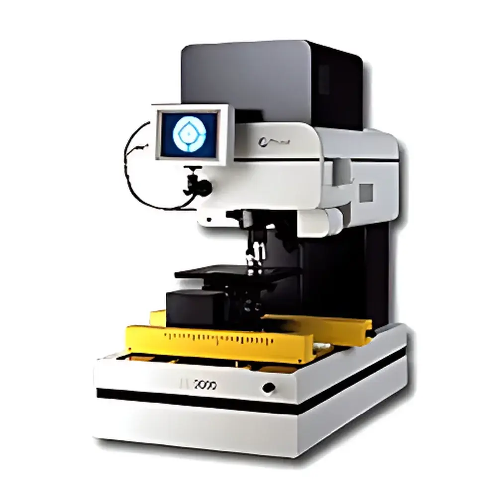
The HalfMoon 0 Reflective Thin-Film Thickness Metrology System is a non-destructive, spectroscopic interferometric measurement platform engineered for high-precision characterization of single- and multi-layer thin films on rigid substrates. Operating on the principle of spectral reflectance analysis, the system acquires full-wavelength reflectance spectra (190–1100 nm) and applies rigorous optical modeling—based on Fresnel equations and matrix formalism—to extract film thickness, refractive index (n), and extinction coefficient (k) simultaneously. Unlike ellipsometric methods requiring polarization control and angular scanning, this instrument delivers rapid, alignment-stable measurements via normal-incidence reflectometry, making it particularly suitable for inline QC environments and R&D labs where throughput, repeatability, and minimal operator intervention are critical. Its modular optical path supports integration with upright or inverted microscopes, enabling spatially resolved metrology down to ~10 µm spot size—essential for patterned wafers, display pixel structures, and localized coating evaluation.
Key Features
- Non-contact, non-invasive measurement—no sample preparation, no surface damage, no vacuum requirement
- Simultaneous determination of thickness and complex refractive index (n + ik) for up to 5-layer stack models
- Extended UV-Vis-NIR spectral coverage (190–1100 nm) with selectable light source configuration (D₂ only, W only, or D₂+W)
- Two operational modes: standard (1 nm – 40 µm) and thick-film optimized (0.8 µm – 250 µm), each calibrated with NIST-traceable reference standards
- Thermoelectrically cooled 512-channel PDA or CCD detector ensures low-noise spectral acquisition and long-term signal stability
- Microscope-compatible optical interface with motorized XYZ stage option (750 VA, AC 100 V ±10 V) for automated wafer mapping and ROI targeting
- Rugged mechanical architecture (96 kg main unit; 714 × 770 × 4810 mm footprint) designed for vibration-insensitive operation in cleanroom and fab-adjacent settings
Sample Compatibility & Compliance
The HalfMoon 0 accommodates flat, optically transparent or semi-transparent substrates including fused silica, BK7 glass, sapphire, silicon wafers (with native oxide or passivation layers), and ITO-coated substrates. It is validated for use on industrially relevant films such as TiO₂, SiO₂, SiNₓ, Al₂O₃, ITO, MoO₃, and organic emissive layers (e.g., NPB, Alq₃) used in OLED fabrication. Measurement uncertainty conforms to ISO 15630-3 for optical thin-film metrology and supports traceability under ISO/IEC 17025 requirements when operated with documented calibration protocols. The system’s software architecture adheres to data integrity principles aligned with FDA 21 CFR Part 11—featuring role-based user authentication, immutable audit trails, electronic signature capability, and secure raw-data archiving.
Software & Data Management
The proprietary MetroSuite™ software provides a validated, Windows-based environment for instrument control, spectral acquisition, optical model construction (including dispersion modeling via Cauchy or Sellmeier functions), and iterative fitting using Levenberg-Marquardt algorithms. All measurement sessions generate timestamped, metadata-rich .mxr files containing raw spectra, fit residuals, confidence intervals for extracted parameters, and version-stamped optical models. Batch processing, map generation (X-Y thickness contours), and export to CSV, XML, or ASTM E2947-compliant report formats are supported. Data backups comply with internal SOPs for GLP/GMP-regulated environments, and optional network deployment enables centralized instrument monitoring across multi-site semiconductor facilities.
Applications
- FPD manufacturing: Thickness uniformity mapping of ITO anodes, SiNx passivation, and color filter AR coatings on TFT-LCD and AMOLED backplanes
- Semiconductor process control: Monitoring gate oxide (SiO₂), high-k dielectrics (HfO₂, ZrO₂), and metal gate stacks during CMOS and compound semiconductor (GaAs, GaN) fabrication
- Optical coating QA: Verification of anti-reflection (MgF₂/SiO₂), high-reflectance (dielectric mirror), and bandpass filter layer sequences
- Magnetic and data storage media: Quantification of CoCrPt-based recording layers and NiFe read-head films on ceramic substrates
- Emerging materials R&D: In-situ characterization of perovskite photovoltaic absorbers, 2D TMDs (MoS₂, WS₂), and ferroelectric HfZrOₓ films
FAQ
What substrate flatness and roughness specifications are required for reliable measurement?
Measurements require root-mean-square (RMS) surface roughness 50 mm over the measurement spot. For moderately rough surfaces (RMS 1–5 nm), optional averaging algorithms and multi-angle compensation routines are available.
Can the system measure absorbing or highly scattering films?
Yes—within physical limits of penetration depth. The software incorporates Kramers-Kronig consistent dispersion models and supports parameter constraints to stabilize fits for strongly absorbing layers (e.g., metals, doped oxides) where k > 0.1 across the measured spectrum.
Is calibration transfer possible between instruments?
Yes—via standardized spectral response characterization using certified reference mirrors and thickness standards. Cross-instrument reproducibility is maintained within ±0.2% thickness deviation for SiO₂ on Si under controlled environmental conditions (23 ± 0.5 °C, 40–60% RH).
Does the system support automated wafer handling integration?
The platform offers SECS/GEM-compliant communication protocols and mechanical interfaces for integration with front-end load ports and robotic handlers in 200 mm and 300 mm fab environments.
How is measurement uncertainty quantified and reported?
Uncertainty budgets follow GUM (JCGM 100:2018) methodology and include contributions from spectral noise, wavelength calibration drift, model assumption error, and substrate optical constant variability—reported as expanded uncertainty (k = 2) in all official test reports.


