Hamamatsu C11665-01 Optical Micrometer for Thin-Film Thickness Measurement
| Brand | Hamamatsu |
|---|---|
| Origin | Japan |
| Manufacturer | Hamamatsu Photonics K.K. |
| Type | Imported Instrument |
| Model | C11665-01 |
| Light Source | LED (940–1000 nm) |
| Measurable Thickness Range (Glass) | 0.5 µm to 700 µm |
| Measurable Thickness Range (Silicon) | 0.5 µm to 300 µm |
| Repeatability (Si, 6 µm film) | ±0.1 nm |
| Accuracy (Si) | ±1 % (within calibration standard traceability) |
| Spot Size | Approx. φ1 mm |
| Working Distance | 5 mm |
| Max. Analyzable Layers | 10 |
| Analysis Methods | FFT-based interference fringe analysis, multi-layer optical modeling, n/k dispersion fitting |
| Measurement Time per Point | 19 ms (acquisition only, excluding computation) |
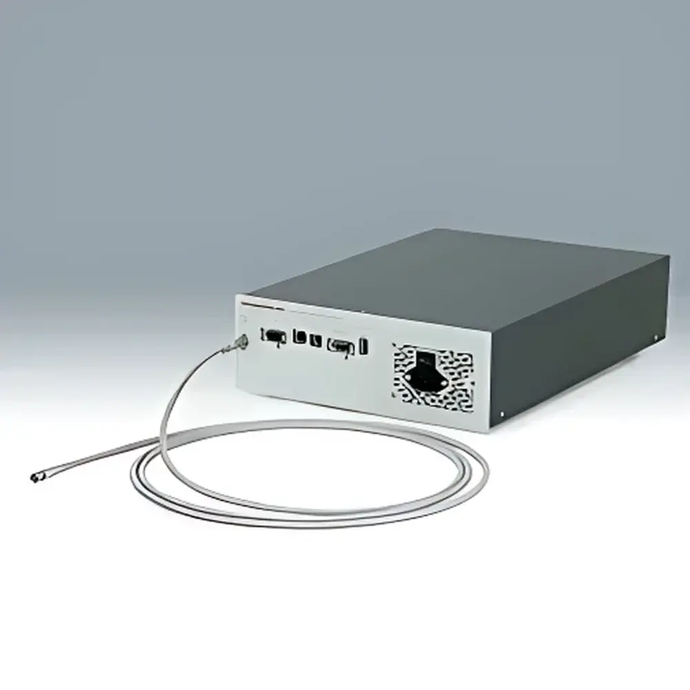
| Fiber Interface | FC-type |
| External Control | RS-232C and Ethernet |
| Power Supply | AC 100–240 V, 50/60 Hz |
| Power Consumption | 85 W |
Overview
The Hamamatsu C11665-01 Optical Micrometer is a compact, integrated interferometric thickness measurement system engineered for non-contact, high-resolution metrology of transparent and semi-transparent thin films on rigid substrates. It operates on the principle of spectral-domain white-light or quasi-monochromatic interference, where reflected light from film interfaces generates interference fringes whose periodicity and phase shift are directly correlated with optical path differences—enabling precise determination of physical thickness and complex refractive index (n, k) dispersion. Designed specifically for semiconductor process control and advanced packaging applications—including through-silicon via (TSV) wafer thinning, dielectric layer monitoring in BEOL integration, and ultra-thin barrier/seed layer qualification—the instrument delivers sub-nanometer repeatability and traceable accuracy across industrially relevant thickness ranges (0.5–300 µm on Si; up to 700 µm on glass/SiO₂). Its monolithic opto-mechanical architecture eliminates alignment drift and external vibration sensitivity, ensuring long-term stability under cleanroom or production-floor conditions.
Key Features
- Self-contained optical head integrating LED source (940–1000 nm), collimation optics, fiber-coupled detection path, and real-time signal processing unit
- Fixed working distance (5 mm) with φ1 mm measurement spot—optimized for flatness-insensitive operation on patterned or slightly warped wafers
- Simultaneous acquisition of spectral interference data enabling robust multi-layer decomposition without prior knowledge of stack composition
- Onboard FFT-based fringe analysis combined with iterative optical modeling for extraction of thickness, surface roughness contribution, and wavelength-dependent n/k values
- Support for up to 10-layer stack modeling with user-definable material dispersion models (Cauchy, Sellmeier, or custom tabulated n/k)
- Low-latency data acquisition (19 ms per point) compatible with automated stage mapping and inline process monitoring integration
- Ruggedized housing rated for Class 1000 cleanroom environments with ESD-safe construction and thermal stabilization circuitry
Sample Compatibility & Compliance
The C11665-01 is validated for quantitative thickness measurement on crystalline silicon (c-Si), fused silica, quartz, sapphire, silicon nitride, silicon dioxide, and polymer-based dielectrics (e.g., polyimide, BCB). It accommodates both bare and metallized substrates, provided the topmost layer exhibits sufficient optical contrast and coherence length compatibility. Measurements comply with ISO 15630-3 (reinforcing steel testing—adapted for optical interferometry traceability), ASTM F1530 (Standard Test Method for Thickness of Transparent Films Using Spectral Interferometry), and support GLP/GMP documentation requirements through audit-trail-enabled software logging. All factory calibrations are NIST-traceable via Hamamatsu’s internal metrology lab accredited to ISO/IEC 17025:2017.
Software & Data Management
Control and analysis are performed via Hamamatsu’s proprietary C11665 Series Software Suite (v3.2+), running on Windows 10/11 64-bit platforms. The software provides full scripting capability (Python API), real-time visualization of interference spectra and modeled fits, batch report generation compliant with FDA 21 CFR Part 11 (electronic signatures, audit trails, role-based access), and seamless export to CSV, HDF5, or industry-standard SEMI E142 (Data Collection Standard) formats. Remote operation via Ethernet supports integration into MES/SCADA systems using Modbus TCP or custom RESTful endpoints. Raw spectral data and fitted parameters are stored with metadata including timestamp, environmental sensor readings (optional ambient temperature/humidity input), and operator ID.
Applications
- Process development and SPC monitoring of Si wafer backgrinding in TSV and 3D IC fabrication
- In-line verification of ALD/CVD-deposited SiO₂, SiNₓ, and HfO₂ gate dielectrics (1–50 nm range with extended modeling)
- Thickness uniformity mapping of photoresist and spin-on-glass (SOG) films across 200 mm and 300 mm wafers
- Characterization of MEMS structural layers (e.g., polysilicon, TiN) during release etch validation
- Quality assurance of optical coatings on laser diode facets and photonic integrated circuit (PIC) waveguides
- Research-grade quantification of 2D material stacks (graphene, MoS₂) on transparent substrates using multi-wavelength extrapolation
FAQ
Does the C11665-01 require reference standards for daily operation?
No—its absolute calibration is maintained via internal wavelength-stabilized LED referencing and factory-characterized optical path compensation. Reference measurements are only required during annual recalibration or after major hardware service.
Can it measure films on curved or non-planar substrates?
It is optimized for flat or gently curved surfaces (radius > 500 mm). For highly contoured parts, optional telecentric objectives or motorized focus tracking modules are available as accessories.
Is the system compatible with vacuum or nitrogen-purged environments?
The base unit is designed for ambient air operation. Vacuum-compatible variants (C11665-01-VAC) with sealed optical paths and feedthrough-rated connectors are offered upon request.
How is measurement uncertainty quantified and reported?
Uncertainty budgets follow GUM (ISO/IEC Guide 98-3) methodology and include contributions from spectral noise, mechanical drift, substrate reflectivity variation, and model assumption error—fully documented in the Certificate of Calibration supplied with each instrument.
What maintenance is required beyond routine cleaning?
Annual performance verification and optical alignment check by Hamamatsu-certified service engineers are recommended. No consumables or recalibration gases are used.