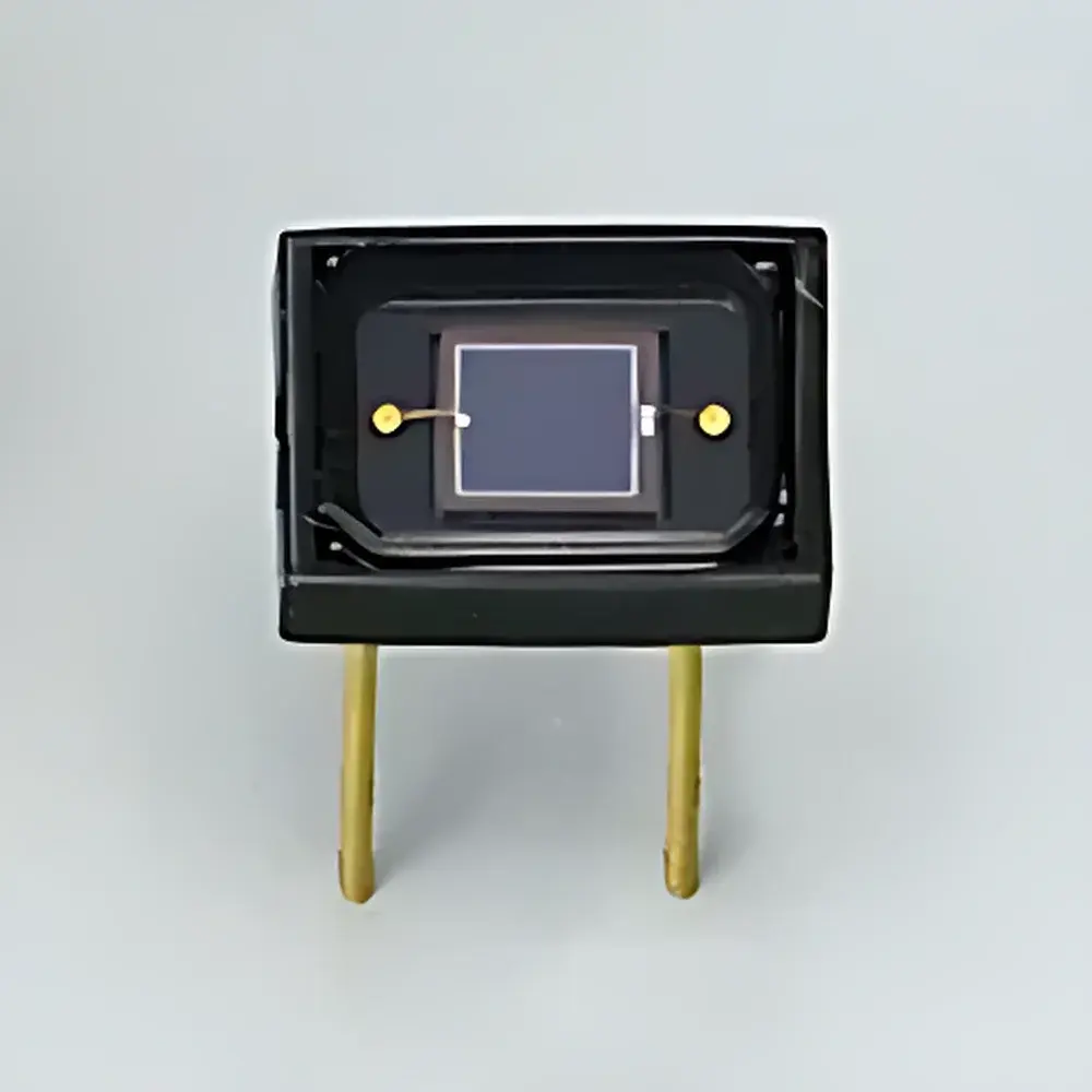
Hamamatsu Silicon Photodiode S1337-33BQ
| Brand | Hamamatsu |
|---|---|
| Origin | Japan |
| Manufacturer Type | Original Equipment Manufacturer (OEM) |
| Product Category | Imported Optical Component |
| Model | S1337-33BQ |
| Component Type | Silicon Photodiode |
| Spectral Range | 190–1100 nm |
| Active Area | 2.4 × 2.4 mm² |
| Peak Wavelength (Typ.) | 960 nm |
| Responsivity (Typ.) | 0.5 A/W @ 960 nm |
| Quantum Efficiency | 75 % @ 200 nm |
| Dark Current (Max.) | 30 pA @ VR = 10 mV |
| Junction Capacitance (Typ.) | 65 pF @ VR = 0 V, f = 10 kHz |
| Rise Time (Typ.) | 0.2 µs @ VR = 0 V |
| Reverse Voltage (Max.) | 5 V |
| Package | Ceramic |
| Cooling | Non-cooled |
| Operating Temperature | Ta = 25 °C (unless specified) |
Overview
The Hamamatsu S1337-33BQ is a high-performance, uncooled silicon photodiode engineered for precision radiometric and photometric measurements across an exceptionally broad spectral range—from deep ultraviolet (190 nm) to near-infrared (1100 nm). Based on single-crystal silicon PIN junction architecture, it delivers high quantum efficiency in the UV region (75% at 200 nm), exceptional linearity over six orders of magnitude of incident optical power, and fast temporal response—making it suitable for applications demanding both spectral fidelity and time-resolved detection. Its 2.4 × 2.4 mm² active area provides optimal signal-to-noise ratio for low-light applications while maintaining spatial uniformity required in calibrated optical setups. Designed and manufactured in Japan under stringent ISO 9001-certified processes, the device features a hermetically sealed ceramic package ensuring long-term stability, humidity resistance, and mechanical robustness in laboratory and industrial environments.
Key Features
- Ultra-high UV quantum efficiency: 75% at 200 nm—significantly exceeding standard Si photodiodes, enabling reliable detection in spectroscopic UV sources and ozone monitoring systems.
- Wide spectral responsivity: Covers 190–1100 nm with peak responsivity of 0.5 A/W at 960 nm—ideal for broadband light source characterization, spectrophotometer reference detectors, and NIR reflectance measurements.
- Low junction capacitance (65 pF typical): Enables high-speed operation with minimal RC time constant limitations—critical for pulsed laser detection and time-of-flight (ToF) applications.
- Fast rise time (0.2 µs typical): Achieved through optimized depletion layer design and low-capacitance packaging—supports modulation frequencies up to several MHz in lock-in or AC-coupled configurations.
- Low dark current (≤30 pA at 10 mV reverse bias): Ensures high dynamic range and measurement accuracy in low-flux conditions, especially relevant for fluorescence lifetime or weak chemiluminescence detection.
- Ceramic TO-5 style package: Provides excellent thermal stability, hermetic sealing, and compatibility with standard optomechanical mounts and vacuum-compatible stages.
Sample Compatibility & Compliance
The S1337-33BQ is compatible with standard photodiode amplifier circuits, transimpedance amplifiers (TIAs), and OEM optical modules operating within ±5 V supply constraints. It complies with RoHS Directive 2011/65/EU and REACH Regulation (EC) No. 1907/2006. While not intrinsically certified for medical or aerospace use, its performance parameters align with test requirements outlined in IEC 60794-1-2 (optical fiber component testing), ASTM E308-22 (computing photometric quantities from spectrophotometric data), and ISO/IEC 17025:2017 (for calibration laboratories using traceable reference standards). The device supports GLP-compliant workflows when integrated into validated instrument platforms—audit trails for calibration coefficients and spectral correction factors can be maintained via external software control.
Software & Data Management
As a passive analog sensing element, the S1337-33BQ does not incorporate embedded firmware or digital interfaces. However, it is fully interoperable with industry-standard data acquisition systems—including National Instruments DAQmx, Keysight U2300A series, and Thorlabs PM100D-compatible power meters—when paired with calibrated transimpedance amplifiers. Hamamatsu provides NIST-traceable spectral responsivity data (in CSV format) covering 190–1100 nm at 1 nm intervals, enabling precise wavelength-dependent correction in spectral analysis software such as MATLAB, Python (using SciPy and NumPy), or LabVIEW-based custom applications. For regulated environments, integration with FDA 21 CFR Part 11-compliant platforms requires external electronic record controls—e.g., timestamped gain calibration logs and user-access audit trails implemented at the system level.
Applications
- UV-VIS-NIR spectrophotometer reference detectors requiring high UV QE and thermal stability.
- Calibration transfer standards in metrology labs performing irradiance and illuminance intercomparisons per CIE S 025/E:2015.
- Optical power monitoring in fiber-coupled laser systems (e.g., 405 nm diode lasers, 850 nm VCSELs, and 1064 nm Nd:YAG harmonics).
- Fluorescence and phosphorescence decay measurement systems where low dark current and sub-microsecond timing are essential.
- Environmental monitoring sensors for solar UV index instrumentation and atmospheric ozone absorption spectroscopy.
- OEM integration into handheld optical analyzers, process control spectrometers, and inline pharmaceutical dissolution testers.
FAQ
Is the S1337-33BQ suitable for vacuum environments?
Yes—the ceramic package is hermetically sealed and rated for operation under high vacuum (≤10⁻⁶ Torr) without outgassing concerns.
What is the recommended reverse bias voltage for optimal linearity?
Operation at 0 V (photovoltaic mode) is recommended for lowest noise and highest linearity; 10 mV bias may be applied for slight speed enhancement without compromising stability.
Does Hamamatsu provide spectral calibration certificates with each unit?
Individual unit calibration is optional (model suffix “-CAL”); standard units ship with batch-level NIST-traceable responsivity curves.
Can this photodiode be used with optical filters for bandpass selection?
Yes—its flat, uncoated silicon surface allows direct mounting of interference filters or dichroic mirrors without adhesive-induced spectral shift.
What is the maximum permissible optical power density before damage onset?
Continuous-wave exposure should remain below 100 mW/mm² at wavelengths >400 nm; for UV (<300 nm), limit to 10 mW/mm² to prevent surface degradation.


