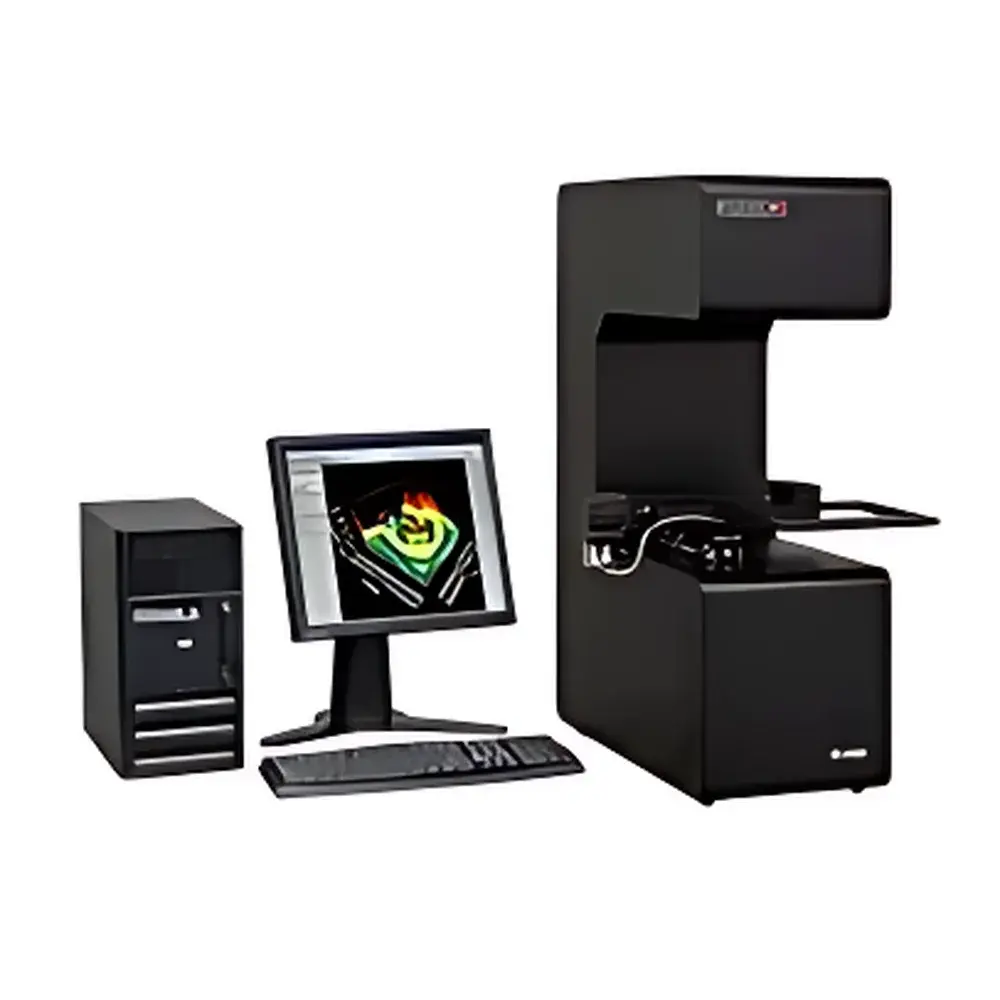
Hinds Instruments 150AT Automated Stress Birefringence Measurement System
| Brand | Hinds Instruments |
|---|---|
| Origin | USA |
| Model | 150AT |
| Retardation Range | 0.005–120+ nm (standard), up to 300+ nm (optional) |
| Retardation Resolution / Repeatability | 0.001 nm / ±0.008 nm (high-precision option) or 0.01 nm / ±0.015 nm (wide-range option) |
| Angular Resolution / Repeatability | 0.01° / ±0.05° (standard) or ±0.07° (wide-range) |
| Measurement Speed | up to 100 points per second (pps), scan time dependent on XY stage parameters |
| Spot Size | 1–3 mm native |
| Light Source Wavelength | 632.8 nm (HeNe, standard) |
| Modulation Frequency | 50 kHz or 50/60 kHz (PEMLabs™ Photoelastic Modulator) |
| Demodulation Method | Signaloc™ Lock-in Amplifier or waveform capture card |
| Measurement Units | nm (retardation), ° (fast-axis angle) |
| Dimensions (H×W×D) | 910 × 415 × 700 mm |
| Compliance | Designed for ISO/IEC 17025-aligned laboratories |
Overview
The Hinds Instruments 150AT Automated Stress Birefringence Measurement System is a precision optical metrology platform engineered for quantitative, non-contact mapping of internal stress-induced birefringence in transparent and semi-transparent materials. Based on the principle of photoelasticity—where mechanical stress induces anisotropic refractive index changes—the system measures linear retardation (in nanometers) and fast-axis orientation (in degrees) across a sample surface using polarized light interferometry coupled with high-frequency photoelastic modulation (PEM) and synchronous lock-in detection. This methodology enables sub-millimeter spatial resolution (<1 mm grid spacing) and nanometer-level retardation sensitivity, making it suitable for both R&D validation and high-throughput production QA/QC workflows in optics, semiconductor, display, and precision injection molding industries.
Key Features
- Motorized X/Y translation stage with programmable scanning trajectories for automated 2D/3D retardation and orientation mapping
- Modular optical architecture supporting native spot sizes from 1–3 mm, scalable to 50 µm with optional high-resolution detector and collimation optics
- Dual measurement modes: high-precision (0.001 nm resolution, ±0.008 nm repeatability at 5 nm retardation) and wide-dynamic-range (0.01 nm resolution, up to 300+ nm retardation)
- Integrated PEMLabs™ photoelastic modulator operating at 50 kHz (or dual 50/60 kHz) for robust noise rejection and signal stability
- Hinds Signaloc™ lock-in amplifier or waveform capture card for real-time demodulation of phase-sensitive signals under varying environmental conditions
- Compact benchtop form factor (910 × 415 × 700 mm) with modular mounting options for integration into cleanroom or inline inspection environments
- Configurable tilt/rotation stages and custom sample holders—including vacuum chucks, thermal stages, and kinematic mounts—for non-planar or temperature-dependent measurements
Sample Compatibility & Compliance
The 150AT accommodates a broad spectrum of optically isotropic and anisotropic materials, including fused silica, BK7 and SF-type optical glasses, sapphire, CaF₂, lithium niobate, single- and polycrystalline silicon wafers, OLED and LCD glass substrates, molded polymer lenses (e.g., PMMA, PC, COC), and pharmaceutical vials. Its measurement protocol aligns with established standards for residual stress evaluation, including ASTM F2129 (for medical device packaging), ISO 10110-5 (optical element stress birefringence specification), and SEMI F20 (silicon wafer flatness and stress characterization). Optional software modules provide traceable calibration logs, user access controls, electronic signatures, and 21 CFR Part 11–compliant audit trails for regulated environments.
Software & Data Management
The system is operated via Hinds’ proprietary measurement suite, offering intuitive graphical interfaces for scan setup, live visualization of retardation maps (color-coded nm contours), fast-axis vector overlays, and cross-sectional profile extraction. Raw data are stored in HDF5 format with embedded metadata (timestamp, instrument configuration, calibration ID, operator ID). Advanced post-processing includes polynomial fitting, Zernike decomposition, stress tensor calculation (via generalized stress-optic law), and batch comparison against reference standards. APIs (DLL and Python bindings) enable integration with MES, LIMS, and factory automation systems. Custom UI skins and report templates (PDF, CSV, XML) can be deployed per customer requirements.
Applications
- Quantification of residual stress gradients in precision optical components prior to coating or assembly
- In-process monitoring of annealing uniformity in float-glass manufacturing and TFT-LCD substrate fabrication
- Failure root-cause analysis of lens delamination, coating adhesion loss, or wafer warpage
- Validation of stress-free bonding in hybrid photonic integrated circuits (PICs)
- Characterization of injection-molded plastic optics for automotive head-up displays (HUDs) and AR/VR waveguides
- Research into thermo-mechanical behavior of novel optical polymers and bio-compatible glass-ceramics
FAQ
What is the minimum measurable retardation and its uncertainty?
The standard configuration achieves 0.005 nm minimum detectable retardation with ±0.008 nm repeatability at low retardation levels (≤5 nm). Uncertainty increases to ±1% of reading above 0.8 nm (high-precision mode) or 1.5 nm (wide-range mode).
Can the system measure curved or tilted surfaces?
Yes—optional motorized tilt/rotation stages and dynamic focus compensation allow accurate mapping on spherical lenses, aspheric elements, and angled substrates without manual re-alignment.
Is spectral or multi-wavelength retardation measurement supported?
Custom configurations integrate tunable lasers or broadband sources with spectrally resolved detection, enabling wavelength-dependent stress analysis and dispersion-corrected birefringence modeling.
How is calibration traceability maintained?
Each system ships with NIST-traceable quarter-wave and half-wave reference plates. Onboard self-calibration routines verify PEM modulation depth, polarization axis alignment, and detector linearity before each measurement session.
Does the software support automated pass/fail decision logic for production screening?
Yes—threshold-based region-of-interest (ROI) masking, statistical process control (SPC) charting, and configurable alarm triggers are embedded in the standard software suite and extensible via scripting.


