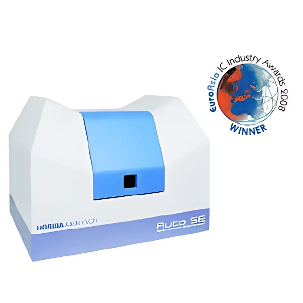
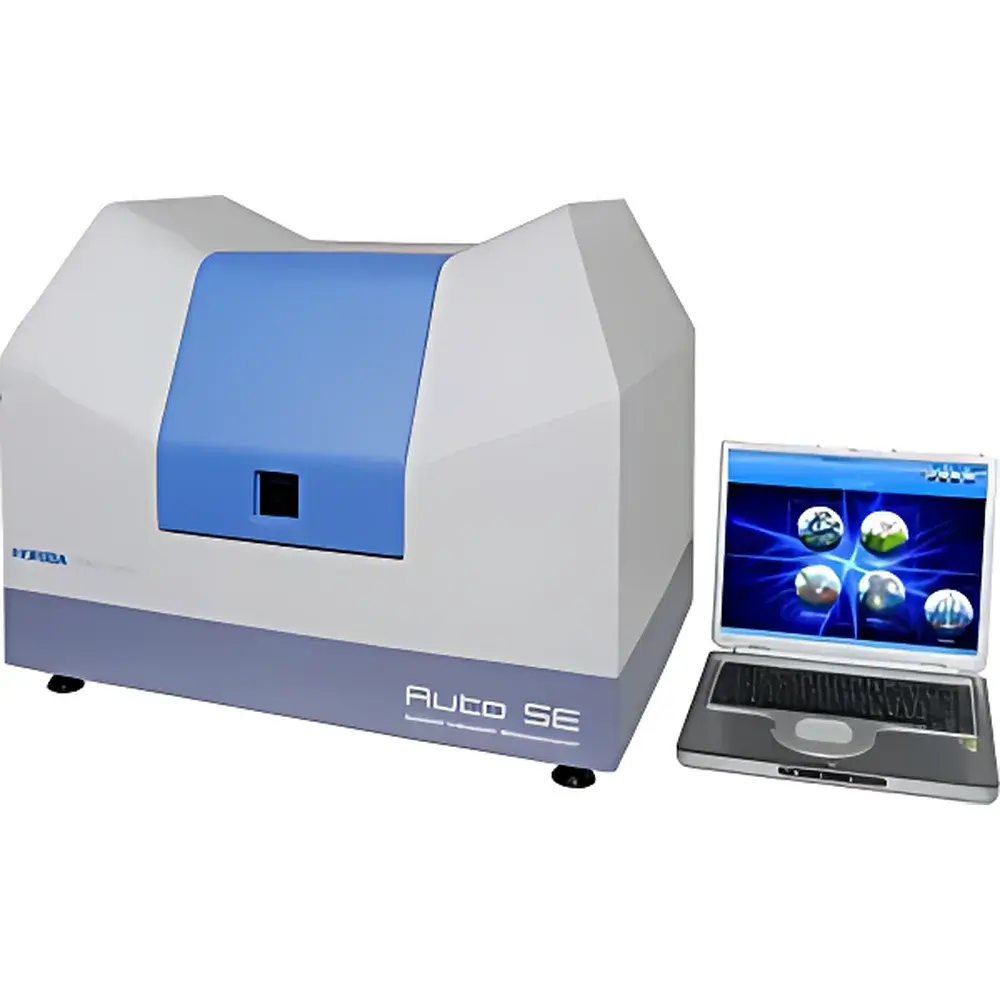
HORIBA Auto SE Automated Spectroscopic Ellipsometer
| Brand | HORIBA |
|---|---|
| Origin | France |
| Model | Auto SE |
| Spectral Range | 450–1000 nm |
| Incident Angle | 70° fixed |
| Detector | CCD array |
| Spot Size Options | 8 discrete sizes (automatically selectable) |
| Sample Stage | Motorized XYZ stage (200 mm × 200 mm travel, Z > 35 mm) |
| Optical Architecture | Liquid crystal phase modulation (no moving parts in measurement path) |
Overview
The HORIBA Auto SE is a fully automated spectroscopic ellipsometer engineered for high-throughput, industrial-grade thin-film metrology. It operates on the fundamental principle of spectroscopic ellipsometry—measuring the change in polarization state of light upon reflection from a sample surface—to extract precise thickness, optical constants (n, k), and compositional information of single- and multilayer thin films. Designed for integration into semiconductor fabrication lines, display manufacturing, photovoltaic R&D, and advanced materials development labs, the Auto SE delivers quantitative, non-contact, and non-destructive analysis with sub-nanometer thickness resolution. Its fixed 70° angle of incidence optimizes sensitivity for common dielectric and semiconductor stacks, while the 450–1000 nm spectral range covers critical absorption edges for Si, SiO₂, SiNₓ, ITO, perovskites, and organic semiconductors. The instrument’s closed-chamber architecture ensures environmental stability and operator safety, meeting ISO 14644-1 Class 8 cleanroom compatibility requirements.
Key Features
- MyAutoView™ patented spot visualization system: Integrated real-time imaging allows direct observation of the measurement spot on any sample surface—regardless of reflectivity, roughness, or pattern density—eliminating positional uncertainty and enabling confident targeting of microstructures, trenches, or heterogeneous regions.
- True one-button operation: From stage positioning to data acquisition, modeling, and report generation, the entire workflow is executed without manual intervention. Measurement time per site is typically under 10 seconds, supporting >100 sites/hour throughput.
- Coaxial confocal micro-spot optics: Eight precisely calibrated spot sizes (ranging from 100 µm) are selected automatically based on user-defined region-of-interest geometry or process recipe—ensuring optimal signal-to-noise ratio and lateral resolution without physical alignment.
- Robust solid-state optical design: Liquid crystal variable retarder (LCVR) modulation replaces mechanical rotating elements, eliminating wear, vibration, and calibration drift. This architecture ensures long-term measurement repeatability (<0.002 ΔΨ, <0.005 ΔΔ over 8 hours).
- Intelligent self-diagnostic engine: Continuous hardware health monitoring detects optical misalignment, lamp intensity decay, detector saturation, or stage positioning errors, and initiates corrective protocols or alerts—reducing scheduled maintenance intervals by up to 60%.
Sample Compatibility & Compliance
The Auto SE accommodates wafers up to 200 mm (8-inch), rectangular substrates (e.g., glass panels, flexible foils), and irregularly shaped research samples. Its motorized XYZ stage supports height variations exceeding 35 mm, enabling measurements across stepped topographies and packaged devices. The enclosed chamber meets CE and IEC 61000-6-3 EMC emission standards. Data integrity complies with FDA 21 CFR Part 11 requirements via audit-trail-enabled software, electronic signatures, and role-based access control—supporting GLP and GMP environments. All measurement models adhere to ASTM E1939 (Standard Guide for Spectroscopic Ellipsometry) and ISO/IEC 17025 traceability frameworks.
Software & Data Management
Equipped with HORIBA’s DeltaPsi² platform, the Auto SE provides intuitive recipe-driven operation, real-time model fitting (with built-in Cauchy, Tauc-Lorentz, Cody-Lorentz, and B-spline dispersion models), and batch reporting in PDF, CSV, and XML formats. Data export supports SML (Standard Metrology Language) for SEMI E137-compliant factory automation interfaces. Version-controlled method libraries, encrypted database storage, and automated backup to network drives ensure compliance with laboratory information management system (LIMS) integration protocols.
Applications
- Semiconductor gate oxide, high-k dielectric, and epitaxial layer thickness uniformity mapping
- Display industry: TFT passivation layers, OLED encapsulation stack characterization
- Photovoltaics: CIGS, perovskite, and silicon heterojunction absorber layer optimization
- Optical coatings: anti-reflection, high-reflection, and filter stack verification
- 2D materials: graphene, MoS₂ monolayer coverage and doping assessment
- Biomedical thin films: hydrogel swelling kinetics and protein adsorption quantification
FAQ
Does the Auto SE support variable angle measurements?
No—the Auto SE uses a fixed 70° incidence angle optimized for maximum sensitivity across a broad range of common thin-film systems. Variable-angle capability is available in HORIBA’s UVISEL+ and SmartSE platforms.
Can it measure transparent substrates like fused silica or sapphire?
Yes—its wide spectral range and high signal-to-noise CCD detection enable accurate modeling of substrate optical constants alongside film properties, provided appropriate reference measurements are included.
Is remote operation and monitoring supported?
Yes—DeltaPsi² includes secure web-based remote desktop access and RESTful API endpoints for integration with MES and SCADA systems.
What level of training is required for routine operation?
Operators require ≤2 hours of hands-on instruction to run standard recipes; advanced modeling and troubleshooting are supported by HORIBA’s certified application engineers and online knowledge base.
How is calibration maintained over time?
The system performs automatic daily reference checks using an integrated NIST-traceable silicon wafer; full recalibration is recommended annually or after major optical component replacement.


