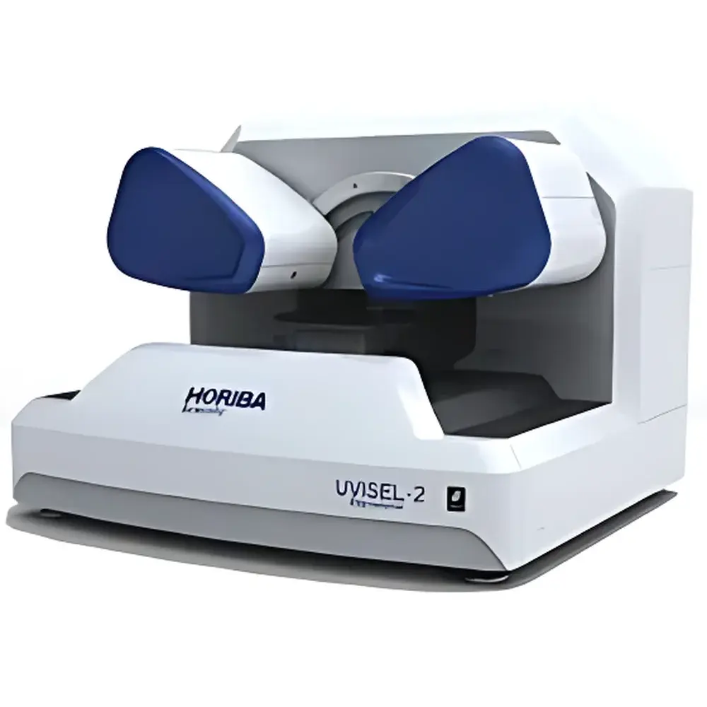
HORIBA Jobin Yvon UVISEL 2 Research-Grade Automated Spectroscopic Ellipsometer
| Brand | HORIBA |
|---|---|
| Origin | France |
| Model | UVISEL 2 |
| Spectral Range | 190–2100 nm |
| Minimum Spot Size | 35 × 85 µm |
| Sample Stage | 200 mm × 200 mm with Motorized XYZ Translation and Auto-Leveling |
| Incidence Angle Range | 35°–90° (Auto-Adjustable, 0.01° Minimum Step) |
| Detector Configuration | Three Independent Detectors (UV-Optimized, VIS-Optimized, NIR-Optimized) |
| Optical Architecture | Dual-Grating Spectrometer with High Stray-Light Suppression |
| Modulation Technology | 50 kHz Photoelastic Modulator (PEM) |
| Imaging Capability | Integrated Visible Microscope with Real-Time Spot Visualization |
| Beam Delivery | Fixed-Path, No Moving Elements in Measurement Light Path |
Overview
The HORIBA Jobin Yvon UVISEL 2 is a research-grade, fully automated spectroscopic ellipsometer engineered for high-precision, non-destructive characterization of thin films and multilayer structures across the deep ultraviolet to near-infrared spectrum (190–2100 nm). It operates on the fundamental principle of spectroscopic ellipsometry—measuring the change in polarization state (ψ and Δ) of light reflected from a sample surface—as a function of wavelength and incidence angle. This enables quantitative determination of optical constants (n, k), layer thicknesses (sub-nanometer resolution), interface roughness, composition gradients, and anisotropy in complex dielectric, semiconductor, organic, and nanostructured materials. Designed for demanding academic, industrial R&D, and process development environments, the UVISEL 2 integrates a fixed-optics PEM-based measurement architecture—eliminating mechanical scanning in the light path—to ensure long-term stability, high reproducibility, and immunity to vibration-induced drift. Its modular detector system—comprising three spectrally optimized detectors—ensures uniform signal-to-noise ratio and photometric linearity across the full spectral range without manual reconfiguration.
Key Features
- High-Fidelity PEM Modulation: 50 kHz photoelastic modulator enables rapid, phase-sensitive detection with no moving parts in the measurement beam path—critical for maintaining calibration integrity during extended acquisition or in vibration-prone laboratory settings.
- Dual-Grating Spectrometer: Engineered for exceptional stray-light suppression (< 10−6 relative intensity), essential for accurate measurement of low-reflectance samples, transparent substrates, and ultra-thin (< 0.5 nm) layers.
- Micro-Spot Versatility: Eight user-selectable spot sizes, down to 35 × 85 µm, with integrated visible microscope imaging for precise targeting—enabling spatially resolved mapping of lateral heterogeneity, patterned devices, and microelectronic features.
- Intelligent Sample Handling: Motorized XYZ stage (200 mm × 200 mm travel) with automatic leveling and Z-axis clearance >35 mm accommodates wafers, glass substrates, flexible films, and irregularly shaped samples; closed-loop feedback ensures repeatable positioning accuracy within ±0.5 µm.
- Automated Optical Alignment: Self-calibrating autofocus, beam centering, and incidence angle verification routines reduce operator dependency and accelerate setup—particularly beneficial for multi-angle or multi-site measurement protocols.
Sample Compatibility & Compliance
The UVISEL 2 supports a broad class of optically anisotropic and isotropic materials—including SiO2, SiNx, ITO, perovskites, polymers, 2D materials (e.g., MoS2, graphene), and biofunctionalized surfaces—on rigid (silicon, sapphire, fused silica) or flexible (PET, PI) substrates. Its variable-angle auto-goniometer (35°–90°, 0.01° resolution) facilitates robust modeling of dispersion-coupled optical responses and critical angle-dependent phenomena such as surface plasmon resonance. The system complies with ISO/IEC 17025 requirements for measurement traceability when operated with NIST-traceable reference standards. Data acquisition and instrument control adhere to GLP/GMP-aligned audit trail functionality (via optional software modules), supporting regulatory submissions under FDA 21 CFR Part 11 where electronic records are required.
Software & Data Management
Controlled by HORIBA’s DeltaPsi2 software suite, the UVISEL 2 provides an integrated environment for experiment design, real-time visualization, advanced optical modeling (including graded interfaces, effective medium approximations, and anisotropic layer stacks), and statistical parameter uncertainty estimation. The software supports batch processing, scripting via Python API, and export of raw ψ/Δ spectra in standardized formats (e.g., .eps, .csv, .mat). All measurement metadata—including instrument configuration, environmental conditions (optional sensor integration), and user annotations—are embedded in data files to ensure full experimental provenance. Version-controlled project archives enable seamless collaboration and long-term data reanalysis across instrument generations.
Applications
- Development and QC of anti-reflective, hard-coat, and barrier coatings for displays and photovoltaics
- Thickness and optical constant monitoring of ALD and CVD-deposited high-k dielectrics and gate stacks
- Quantification of interfacial oxidation and native oxide growth kinetics on semiconductor surfaces
- Characterization of organic thin-film transistors (OTFTs), OLED emissive layers, and perovskite solar cell architectures
- In-situ and real-time ellipsometry for plasma etch endpoint detection and atomic layer etching process control
- Non-contact metrology of 2D material monolayers and van der Waals heterostructures
FAQ
What is the minimum measurable film thickness with the UVISEL 2?
The theoretical lower limit depends on material contrast and measurement configuration, but sub-angstrom thickness resolution is routinely achieved for high-index contrast systems (e.g., SiO2/Si) using multi-angle, multi-wavelength analysis.
Can the UVISEL 2 measure transparent conductive oxides on glass?
Yes—the system’s wide spectral coverage (190–2100 nm) and dual-grating stray-light rejection enable accurate modeling of both absorption edge and interference fringes in ITO, AZO, and FTO films on soda-lime or borosilicate glass.
Is vacuum or purged operation required for UV measurements?
For measurements below ~195 nm, nitrogen purging or vacuum operation is recommended to mitigate atmospheric O2 and H2O absorption; the UVISEL 2 is compatible with standard purge enclosures and vacuum-compatible sample stages.
Does the system support in-situ measurements?
Yes—modular flange options and compact optical head design allow integration into load-lock chambers, gloveboxes, and thermal/controlled-atmosphere stages for real-time thin-film growth or environmental response studies.
How is calibration maintained over time?
The system employs internal reference channels and automated alignment checks; annual recalibration against certified reference samples (e.g., Si/SiO2 wafers) is recommended to maintain traceability to SI units per ISO/IEC 17025 guidelines.


