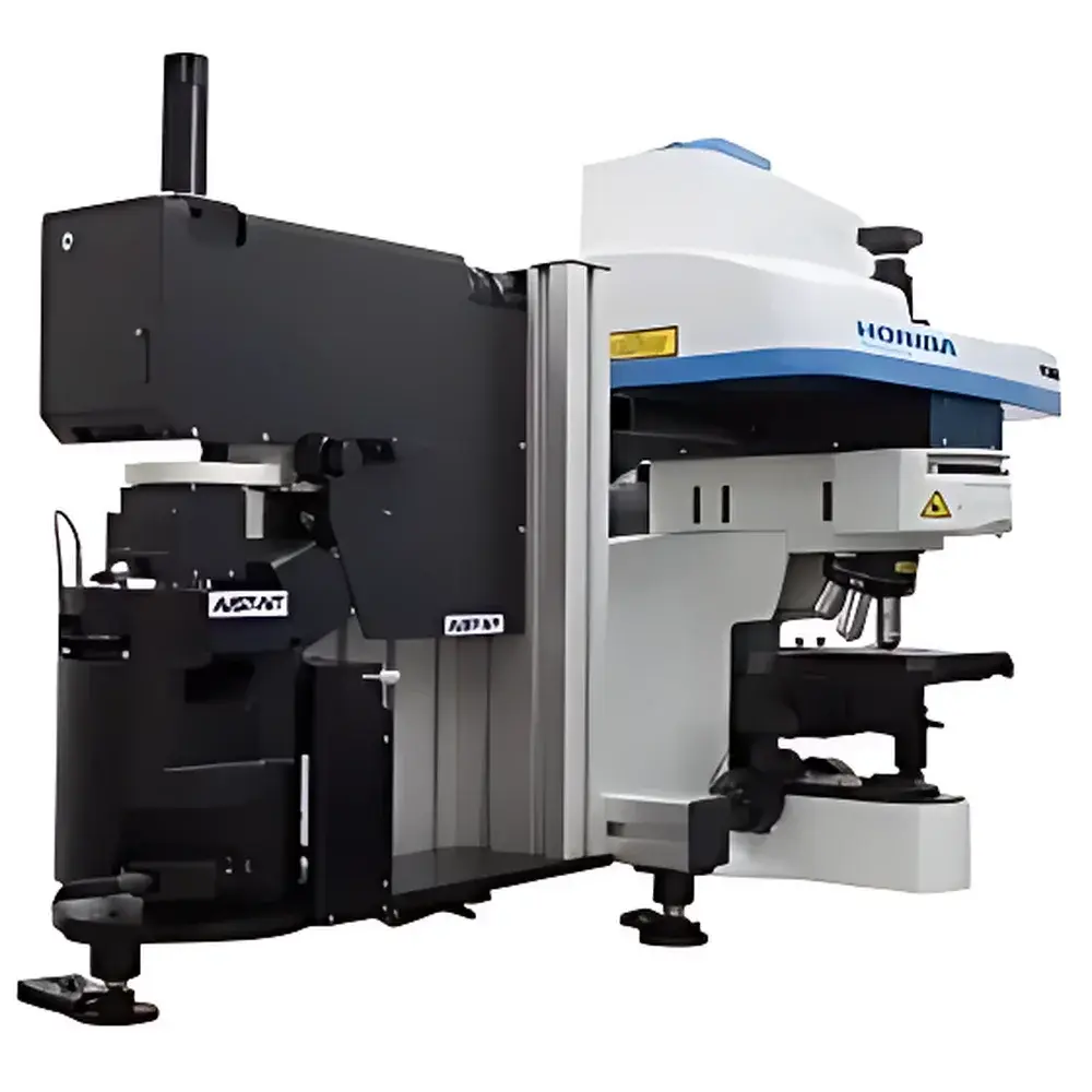
HORIBA Nano XploRA AFM-Raman Coupling System
| Brand | HORIBA |
|---|---|
| Origin | France |
| Manufacturer Type | Authorized Distributor |
| Import Status | Imported |
| Model | Nano XploRA |
| Instrument Type | Confocal Micro-Raman Spectrometer with Integrated Atomic Force Microscopy (AFM) |
| Optical Coupling Options | Top, Side, and Bottom Illumination Paths |
| Objective Compatibility | Supports High-NA ×100 Objectives for All Coupling Modes |
| TERS-Ready Architecture | Fully Optimized for Tip-Enhanced Raman Scattering |
| AFM Feedback | Automatic Laser Alignment via Photodiode-Based Optical Lever System |
| Scan Head | High-Frequency, Low-Noise Piezoelectric Scanner |
| Software Integration | Unified Control Suite for Synchronized AFM Topography, Mechanical Mapping, and Point/Line/Area Raman Spectroscopy |
| Compliance Framework | Designed to Support GLP/GMP workflows with audit-trail-capable data logging (21 CFR Part 11-ready configuration available) |
Overview
The HORIBA Nano XploRA AFM-Raman Coupling System is a fully integrated, confocal micro-Raman spectrometer engineered for synchronized atomic force microscopy and vibrational spectroscopic analysis at the nanoscale. It operates on the principle of confocal laser excitation combined with precise spatial registration between AFM topographic feedback and Raman spectral acquisition—enabling true co-localized measurement of nanomechanical, topographic, and chemical properties within a single instrument platform. Unlike conventional sequential or loosely coupled systems, the Nano XploRA implements hardware-level synchronization between the AFM scan controller and the Raman spectrometer’s CCD readout, ensuring sub-pixel spatial fidelity (<50 nm lateral registration accuracy under standard conditions) and eliminating drift-induced misalignment during long-duration mapping. The system leverages HORIBA’s decades of expertise in high-throughput Raman optics and robust SPM interfacing architecture, supporting both far-field confocal Raman imaging and near-field tip-enhanced Raman scattering (TERS) modalities without hardware reconfiguration.
Key Features
- Triple optical coupling geometry: top, side, and bottom illumination paths—each compatible with ×100, high-numerical-aperture (NA > 0.9) objectives to maximize Raman photon collection efficiency across transparent, opaque, and tilted-tip configurations.
- Automated optical lever alignment: real-time photodiode-based feedback ensures stable AFM laser positioning on the cantilever, minimizing thermal drift and operator intervention during extended acquisitions.
- High-frequency, low-noise piezoelectric scan head: engineered for stability against acoustic and vibrational perturbations common in shared laboratory environments; supports scanning speeds up to 10 Hz line rate with <0.5 nm RMS noise floor in open-loop mode.
- TERS-optimized mechanical design: rigid, kinematically aligned optical path with minimized degrees of freedom; includes precision XYZ nanopositioning stage for tip-sample distance control and active laser focus tracking.
- Unified software architecture: single GUI for simultaneous control of AFM imaging modes (contact, tapping, phase, amplitude, force-distance), Raman spectral acquisition (point, line, area, hyperspectral), and cross-correlated data export in standardized formats (e.g., HDF5, JCAMP-DX, SPIP-compatible).
Sample Compatibility & Compliance
The Nano XploRA AFM-Raman platform accommodates a broad range of solid-state samples—including 2D materials (graphene, MoS₂, h-BN), semiconductor nanostructures (quantum dots, nanowires), polymer thin films, biological membranes, and catalytic nanoparticles—without requiring conductive coating or vacuum compatibility. Its modular optical interface allows integration with third-party AFM controllers (e.g., Bruker, Park Systems, Asylum Research) while maintaining full spectral calibration traceability per ISO/IEC 17025 guidelines. For regulated environments, optional 21 CFR Part 11-compliant software modules provide electronic signatures, audit trails, and role-based access control—fully aligned with GLP and GMP documentation requirements. All Raman calibrations are referenced to NIST-traceable standards (e.g., silicon Raman peak at 520.7 cm⁻¹), and spectral reproducibility is validated per ASTM E1840-22 for micro-Raman instrumentation.
Software & Data Management
HORIBA’s LabSpec 6 software suite provides native support for AFM-Raman correlation workflows, including automatic overlay of topographic height maps onto Raman intensity or peak position maps, multivariate analysis (PCA, cluster analysis), and spectral deconvolution using constrained Voigt fitting. Raw datasets are stored in vendor-neutral HDF5 containers with embedded metadata (laser wavelength, objective NA, grating, integration time, AFM setpoint, etc.), enabling interoperability with Python-based analysis pipelines (e.g., SciPy, scikit-learn, PySPM). Batch processing scripts allow automated generation of chemical contrast maps from large-area hyperspectral cubes (>10⁴ spectra), with built-in tools for cosmic ray removal, fluorescence background subtraction, and wavenumber calibration validation. Export options include TIFF stacks for image analysis platforms (ImageJ/Fiji), CSV for spreadsheet-based quantification, and MTEX-compatible formats for crystallographic orientation mapping.
Applications
- Layer-number identification and strain mapping in few-layer 2D materials via correlated G- and 2D-band Raman shifts and AFM step-height measurements.
- Nanoscale defect characterization in carbon nanotubes and graphene—combining AFM-derived topographic discontinuities with D/G intensity ratios and phonon lifetime analysis from Raman linewidths.
- In situ electrochemical AFM-Raman studies of battery electrode interfaces, where local SEI formation is tracked chemically (via C–F, Li–O, or P–F Raman bands) while concurrently monitoring surface modulus changes via AFM contact resonance.
- TERS-enabled molecular fingerprinting of single biomolecules (DNA origami, amyloid fibrils) with spatial resolution down to 2 nm—leveraging plasmonically enhanced tips and polarization-resolved detection.
- Quality control of semiconductor heterostructures, correlating AFM-measured roughness (Rq, Ra) with Raman-derived composition gradients (e.g., SiGe alloy fraction via Ge–Ge vs. Si–Si peak intensities).
FAQ
Can the Nano XploRA be retrofitted to an existing AFM system?
Yes—HORIBA offers turnkey integration kits for major AFM platforms, including mechanical mounting fixtures, optical path adapters, and synchronized trigger I/O modules compatible with standard TTL and LVDS timing protocols.
What is the typical spatial resolution achievable in TERS mode?
Under optimized conditions (sharp Au-coated tips, resonant excitation, stable tunneling current), lateral resolution of 2–5 nm is routinely achieved; practical resolution in ambient or liquid environments typically ranges from 10–20 nm depending on tip quality and signal-to-noise ratio.
Is fluorescence suppression supported?
Yes—the system includes notch and edge filters optimized for 532 nm, 638 nm, and 785 nm excitation, as well as optional time-gated detection modules for fluorescence lifetime discrimination.
How is spectral calibration maintained during long-term operation?
An internal reference laser diode and automated silicon wafer calibration routine run at user-defined intervals (e.g., before each session or hourly), ensuring wavenumber accuracy better than ±0.2 cm⁻¹ over 8-hour acquisitions.
Does HORIBA provide application-specific method development support?
Yes—HORIBA Scientific’s Applications Lab offers remote and on-site method optimization, including TERS tip selection guidance, optimal laser power balancing, and multivariate spectral interpretation training tailored to materials science, life science, or semiconductor use cases.
Related Products