ISDI Haoliang-Series Ultra-Large-Format CMOS Image Sensor
| Origin | Imported |
|---|---|
| Manufacturer Type | Distributor |
| Model | Haoliang. |
| Image Resolution | Customizable up to 120 MP (e.g., 16,384 × 7,680) |
| Pixel Size | 50 µm or 100 µm (selectable) |
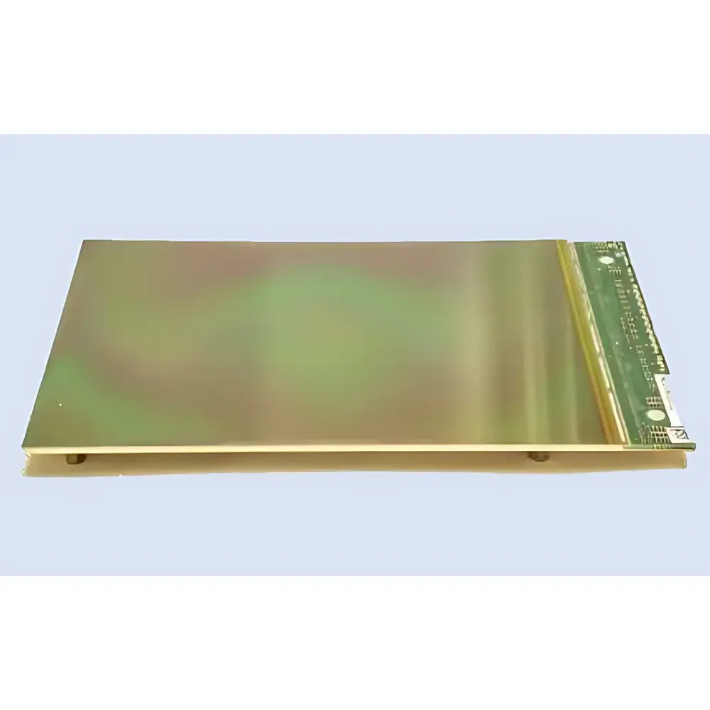
| Active Chip Area | Up to 82 mm × 39 mm (wafer-level tiling supported) |
| On-Sensor Memory | 36 GB DDR4 buffer integrated on sensor carrier PCB |
| Readout Speed | Up to 40 fps at full resolution (configurable via ROI and binning) |
| Dynamic Range | ≥85 dB (typical, 16-bit linear output) |
| Quantum Efficiency | >90% at 550 nm (back-illuminated, thinned silicon) |
Overview
The ISDI Haoliang-Series Ultra-Large-Format CMOS Image Sensor is a wafer-scale monolithic or tiled imaging solution engineered for scientific, industrial, and synchrotron-grade applications requiring exceptional spatial continuity, low-noise performance, and radiation-tolerant operation. Unlike conventional mosaic-based large-area detectors, the Haoliang architecture leverages ISDI’s proprietary low-noise pixel design—featuring deep-depletion, back-illuminated silicon with optimized charge collection efficiency—to deliver high quantum efficiency (>90% at 550 nm) and sub-electron read noise across the entire active area. The sensor operates on a rolling shutter principle with precise timing control, supporting both global reset and non-destructive readout modes. Its physical layout accommodates seamless tiling via mechanical and electrical alignment features, enabling continuous imaging fields exceeding 100 mm in width without optical or electronic stitching artifacts. Designed from inception for integration into X-ray indirect-detection systems—including coupling to fiber-optic plates (FOP) or direct scintillator deposition—the Haoliang sensor maintains stable performance under moderate ionizing radiation exposure, making it suitable for beamline instrumentation, EUV metrology, and high-energy physics experiments.
Key Features
- Wafer-level scalable architecture: Supports monolithic fabrication or precision-aligned tiling to form contiguous imaging areas up to 160 mm × 40 mm.
- Back-illuminated, deep-depletion silicon: Optimized for high QE (>90% peak), low dark current (<0.1 e⁻/pixel/s at −20°C), and minimal etaloning in NIR.
- Dual full-well capacity modes: Selectable High Full-Well (HFW: ~100 ke⁻) and Low Full-Well (LFW: ~15 ke⁻) configurations for dynamic range adaptation across low-light and high-flux regimes.
- On-die temperature sensor with ±0.5°C accuracy: Enables real-time thermal drift compensation and closed-loop cooling control.
- Programmable Region-of-Interest (ROI): Hardware-accelerated ROI selection down to 16 × 16 pixels with independent gain, offset, and integration time control.
- Non-destructive readout (NDRO) mode: Allows multiple sampling of the same integration cycle for noise reduction and photon counting validation.
- Flexible digital interface: LVDS or Sub-LVDS output compliant with Camera Link HS, CoaXPress 2.0, or custom FPGA/ASIC integration; supports trigger-in, trigger-out, and strobe synchronization.
Sample Compatibility & Compliance
The Haoliang sensor is qualified for integration with fiber-optic faceplates (FOPs) of thicknesses ranging from 3 mm to 12 mm, as well as with directly deposited CsI:Tl, Gd₂O₂S:Tb, or LuAG:Ce scintillation layers. Its passivation stack meets MIL-STD-883H Class H requirements for humidity resistance and particle contamination control. All variants are RoHS 3 and REACH compliant. For regulated environments—including clinical preclinical imaging and GLP-compliant materials characterization—the sensor’s deterministic readout architecture and traceable calibration metadata support audit-ready documentation per ISO/IEC 17025 and FDA 21 CFR Part 11 when deployed with validated acquisition firmware.
Software & Data Management
ISDI provides the Haoliang SDK—a cross-platform C/C++ API with Python bindings—for low-level register access, timing configuration, and streaming control. Acquisition software includes ISDI Capture Studio (Windows/Linux), which supports real-time histogram analysis, flat-field correction, bad-pixel mapping, and TIFF/HDF5 export with embedded EXIF-style metadata (exposure, temperature, ROI coordinates, sensor ID). Raw frame buffers are timestamped with <100 ns jitter using PTPv2-compatible hardware clocks. Optional firmware modules enable on-sensor histogram accumulation, centroid calculation, and lossless compression (JPEG-XR or FIC) to reduce host-side bandwidth demand.
Applications
- Synchrotron X-ray diffraction and tomography: Continuous field-of-view imaging with sub-micron spatial registration stability over multi-hour acquisitions.
- EUV lithography mask inspection: High-dynamic-range capture of defect contrast against reflective multilayer backgrounds.
- Astronomical focal plane arrays: Tiled configurations for wide-field survey instruments operating at cryogenic temperatures (−40°C operational limit).
- High-speed industrial CT: Synchronized multi-sensor acquisition with microsecond-level inter-frame jitter control.
- Neutron radiography: Scintillator-coupled operation with neutron-induced background suppression via pulsed illumination gating.
FAQ
Is the Haoliang sensor available in both 50 µm and 100 µm pixel pitch variants?
Yes—both pixel sizes are offered as standard configurations. The 50 µm variant prioritizes spatial resolution and is typically used in microscopy and metrology; the 100 µm version emphasizes sensitivity and full-well capacity for low-flux X-ray applications.
Can the sensor be operated in vacuum or controlled inert-gas environments?
Yes. The ceramic LCC package and hermetic die attach process qualify the sensor for operation in dry nitrogen or argon atmospheres down to 10⁻³ mbar. Vacuum compatibility requires optional getter integration and is subject to qualification testing.
Does ISDI provide calibration data with each sensor shipment?
Each unit ships with a NIST-traceable calibration report including dark current maps, PRNU (Photo Response Non-Uniformity) coefficients, gain/offset tables per ROI mode, and QE curve measured at five wavelengths (400–900 nm).
What cooling options are supported?
The sensor carrier board includes thermal vias and mounting holes compatible with Peltier coolers (−20°C to +40°C setpoint) or liquid cold plates. A dedicated thermal interface material (TIM) pad is specified for optimal heat transfer.
Is FPGA reference design available for custom interface development?
Yes—ISDI provides a complete VHDL/Verilog reference design for Xilinx Kintex Ultrascale+ and Intel Stratix 10 platforms, including PCIe Gen3 DMA controllers, real-time ROI parser logic, and error-correcting code (ECC) for memory buffers.


