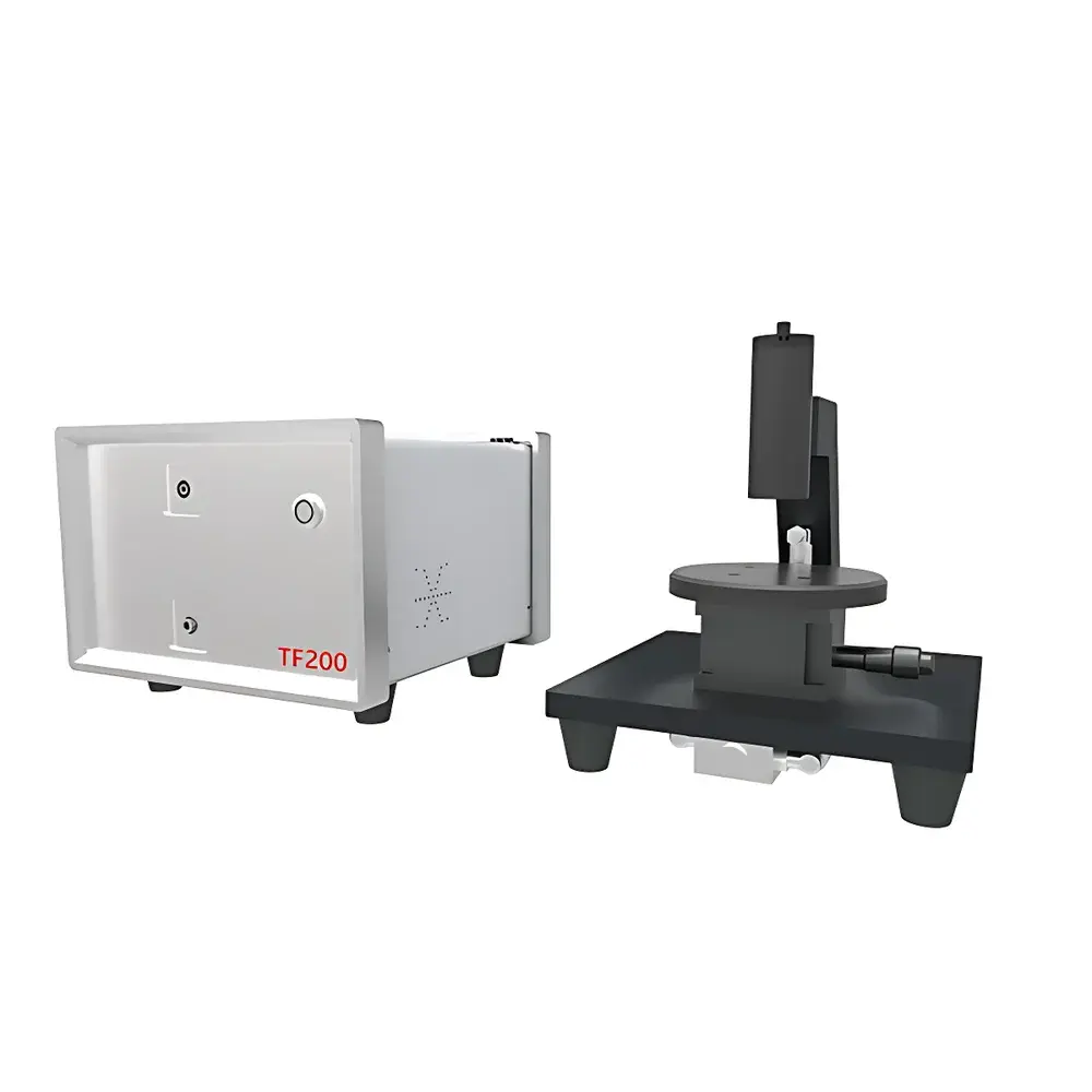
KJ GROUP TF200 Thin Film Thickness Measurement System
| Brand | KJ GROUP |
|---|---|
| Origin | Liaoning, China |
| Manufacturer Type | Authorized Distributor |
| Country of Origin | China |
| Model | TF200 |
| Pricing | Available Upon Request |
| Wavelength Ranges | TF200-VIS: 380–1050 nm |
| TF200-EXR | 380–1700 nm |
| TF200-DUV | 190–1100 nm |
| TF200-XNIR | 900–1700 nm |
| Thickness Range | 1 nm – 3 mm (model-dependent) |
| Accuracy | Max(0.4% of thickness, 2 nm) for TF200-VIS/EXR/DUV |
| Precision | 0.2 nm (VIS/EXR/DUV), 3 nm (XNIR) |
| Incidence Angle | 90° (normal incidence) |
| Sample Compatibility | Transparent or semi-transparent films |
| Measurement Modes | Reflectance and transmittance |
| Spot Size | 2 mm (optional micro-spot accessory available) |
| In-line Capability | Yes |
| Scanning Options | XY motorized stage (optional) |
Overview
The KJ GROUP TF200 Thin Film Thickness Measurement System is a non-contact, optical interferometry-based metrology platform engineered for high-precision, real-time characterization of single- and multi-layer thin film structures. Operating on the principle of spectral reflectance interference, the system illuminates the sample with broadband light and analyzes the wavelength-dependent phase shifts in the reflected (and optionally transmitted) signal. By fitting the measured interference spectrum to a physically constrained optical model—including layer stack geometry, dispersion-corrected refractive index (n) and extinction coefficient (k) profiles—the TF200 computes film thickness with sub-nanometer resolution. Its modular optical architecture supports four dedicated configurations—TF200-VIS, TF200-EXR, TF200-DUV, and TF200-XNIR—each optimized for distinct spectral windows and application-specific thickness regimes. Designed for integration into both laboratory and production environments, the TF200 delivers traceable, repeatable measurements without surface contact, sample preparation, or vacuum requirements.
Key Features
- Multi-spectral platform with four interchangeable optical modules covering deep ultraviolet (190 nm) to extended near-infrared (1700 nm)
- Simultaneous determination of thickness, refractive index (n), and extinction coefficient (k) for films ≥100 nm
- Normal-incidence (90°) optical geometry ensuring minimal angular sensitivity and simplified calibration
- Sub-nanometer precision (0.2 nm typical for VIS/EXR/DUV variants) and accuracy defined by max(0.4% of measured thickness, 2 nm)
- Support for both reflectance-only and combined reflectance/transmittance analysis to resolve ambiguity in symmetric stacks
- Motorized XY scanning stage option enabling automated mapping of thickness uniformity across wafers or display substrates
- Micro-spot probe accessory (2 mm standard spot; optional reduced-diameter optics) for localized measurement on patterned or heterogeneous surfaces
- In-line ready design with Ethernet and digital I/O interfaces for integration into semiconductor fab toolsets or roll-to-roll coating lines
Sample Compatibility & Compliance
The TF200 accommodates transparent and semi-transparent dielectric and semiconductor thin films on rigid or flexible substrates—including SiO₂, SiNₓ, photoresists, ITO, polyimide, DLC, parylene, and AR coatings. It is routinely deployed in environments governed by ISO/IEC 17025, ASTM E2375 (standard guide for optical measurement of thin film thickness), and SEMI D39 (specifications for optical thin film metrology tools). While not FDA-certified as standalone hardware, its data output structure and audit-trail-capable software support alignment with FDA 21 CFR Part 11 requirements when deployed under validated laboratory information management systems (LIMS) or electronic lab notebooks (ELN). All factory calibrations are traceable to NIST-standard reference materials.
Software & Data Management
The TF200 operates with KJ GROUP’s proprietary SpectraFilm™ software, a Windows-based application providing full control over acquisition parameters, optical modeling, and report generation. The software includes built-in libraries of optical constants for >200 common thin film materials and supports user-defined dispersion models (Cauchy, Sellmeier, Tauc-Lorentz). Each measurement session records raw spectra, fitted parameters, residuals, and confidence metrics. Data export formats include CSV, XML, and PDF reports compliant with GLP/GMP documentation standards. Version-controlled software updates and encrypted project file storage ensure data integrity across multi-user laboratories. Optional API access enables integration with MES or SCADA platforms for automated process feedback loops.
Applications
- Semiconductor manufacturing: Thickness control of gate oxides (SiO₂), hard masks (SiNₓ), photoresist layers, SOI handle wafers, and MEMS structural films
- Flat panel display production: Liquid crystal cell gap verification, ITO electrode uniformity mapping, and PI alignment layer thickness validation
- LED and microLED fabrication: Epitaxial layer monitoring, passivation film QC (e.g., Al₂O₃, SiO₂), and phosphor coating thickness
- Touch sensor and AR/VR optics: ITO patterning verification, anti-reflective stack composition analysis, and multilayer interference filter characterization
- Automotive and medical device coating: DLC hardness layer thickness, anti-fog polymer coatings, and drug-eluting parylene C/D coatings on balloon catheters
FAQ
Does the TF200 require vacuum or environmental chamber operation?
No. The system operates under ambient atmospheric conditions and does not require vacuum pumping or temperature-controlled enclosures for standard measurements.
Can the TF200 measure opaque or highly absorbing films?
It is optimized for transparent and semi-transparent films. Opaque metal layers (e.g., thick Al, Cu) cannot be directly measured unless used as reflective backplanes in transparent stacks amenable to transmittance analysis.
Is calibration required between different material types?
Factory calibration is substrate-agnostic; however, accurate n/k determination requires initial optical constant input or iterative fitting using known reference samples. A one-time empirical calibration is recommended for high-volume production of identical film stacks.
What level of training is needed to operate the TF200?
Basic operation requires less than one day of instruction. Advanced modeling, dispersion fitting, and multi-layer deconvolution benefit from foundational knowledge in thin film optics—training modules and application notes are included with the system.
How is measurement uncertainty quantified in the TF200 software?
Uncertainty is reported per measurement as a composite value derived from spectral noise floor, model convergence residuals, and propagation of n/k parameter sensitivity—fully documented in the exported analysis log.


