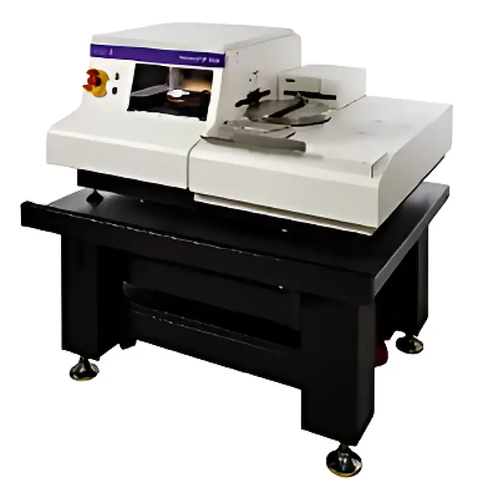
KLA P-170 Capacitive Profilometer
| Brand | KLA |
|---|---|
| Origin | Malaysia |
| Manufacturer Type | Authorized Distributor |
| Origin Category | Imported |
| Model | P-170 |
| Pricing | Available Upon Request |
| Measurement Principle | Capacitive Sensing |
| Measurement Range | 0–1000 µm |
| Accuracy | ±0.5 nm |
| Probe Tip Radius | 2.0 µm |
| Probe Normal Force | 0.5–50 mg |
| Scan Length | Up to 200 mm (Seamless, No Stitching Required) |
| Step Height Repeatability | 0.4 nm |
| Vertical Resolution | 0.001 nm |
| Maximum Sample Size | 200 mm Diameter |
Overview
The KLA P-170 Capacitive Profilometer is a high-precision, non-optical surface metrology system engineered for nanoscale step height and topographic characterization of semiconductor wafers, MEMS devices, thin-film stacks, photomasks, and advanced packaging substrates. Utilizing a closed-loop capacitive displacement sensor coupled with a mechanically stabilized diamond-tipped probe, the P-170 delivers direct, material-independent vertical measurements—eliminating optical interference effects common in interferometric or confocal systems. Its core architecture integrates a low-noise, high-bandwidth feedback control loop that dynamically maintains constant probe-sample interaction force across varying surface topographies, ensuring consistent contact mechanics and minimizing plowing artifacts. Designed for integration into automated fab environments, the P-170 supports full wafer handling from 75 mm to 200 mm diameter—including transparent (e.g., fused silica, quartz) and opaque (Si, GaAs, SiC) substrates—with auto-alignment and vacuum chucking. The system operates under cleanroom-compatible environmental controls and meets mechanical stability requirements per SEMI S2 and ISO 14644-1 Class 5 specifications.
Key Features
- Capacitive sensing architecture enabling sub-angstrom vertical resolution (0.001 nm) and exceptional step height repeatability (0.4 nm RMS over 100 repeated measurements)
- Seamless 200 mm single-pass scanning capability—no image stitching required—ensuring spatial coherence and eliminating registration errors inherent in tiled acquisitions
- Automated force control system maintaining probe normal load between 0.5 mg and 50 mg, dynamically adjusted in real time to preserve tip integrity and measurement fidelity on soft polymers or hard ceramics
- Diamond probe with 2.0 µm nominal tip radius, certified per ISO 11549-3; interchangeable stylus options available for specialized applications (e.g., ultra-low-force polymer profiling)
- Integrated SECS/GEM interface compliant with SEMI E30 and E40 standards, enabling seamless communication with factory host systems and MES platforms
- Full-auto sequencing engine supporting pattern recognition-based site selection, multi-site navigation, and conditional measurement logic (e.g., “measure only if feature width > 5 µm”)
Sample Compatibility & Compliance
The P-170 accommodates flat, rigid substrates up to 200 mm in diameter and ≤10 mm thick, including silicon, sapphire, glass, quartz, metal-coated wafers, and low-k dielectric films. It supports both conductive and insulating surfaces without signal degradation—critical for measuring resistive TSV liners or high-k gate oxides. The system complies with ISO/IEC 17025 calibration traceability requirements when operated with KLA-certified reference standards (e.g., NIST-traceable step height artifacts SRM 2162). All measurement protocols adhere to ASTM E2228 (Standard Test Method for Measuring Step Heights Using Contact Profilometers) and are compatible with GLP/GMP audit trails when paired with KLA’s validated software suite.
Software & Data Management
Operation is managed via KLA’s proprietary WinStep™ software platform, version 5.3 or later, which provides ISO 17025-compliant data acquisition, analysis, and reporting workflows. The software includes built-in statistical process control (SPC) modules, cross-section extraction, power spectral density (PSD) analysis, and ISO 25178 surface texture parameter calculation (Sa, Sq, Sz, etc.). Audit trail functionality records all user actions, parameter changes, and calibration events in tamper-evident format, satisfying FDA 21 CFR Part 11 electronic record requirements. Raw profilometry data is stored in vendor-neutral .xyz ASCII format and can be exported to MATLAB, Python (NumPy), or industry-standard metrology databases (e.g., Applied Materials DMS, PDF Solutions Exensio).
Applications
- Quantitative evaluation of etch depth uniformity and profile angle in BEOL interconnect structures
- Thickness verification of spin-on carbon (SOC) and BARC layers prior to lithography
- Characterization of CMP dishing and erosion on shallow trench isolation (STI) and copper damascene structures
- 3D reconstruction of MEMS cantilevers, RF resonators, and microfluidic channel geometries
- Validation of nanoimprint lithography (NIL) fidelity and residual layer thickness (RLT)
- Post-deposition film stress analysis via substrate curvature measurement using multi-point bow mapping
FAQ
What is the minimum measurable step height on the P-170?
The system reliably resolves steps ≥0.1 nm in controlled environments, with guaranteed repeatability down to 0.4 nm per ASTM E2228 Annex A2.
Can the P-170 measure transparent substrates such as fused silica or CaF₂?
Yes—the capacitive sensing principle is independent of optical transmission or reflectivity, enabling accurate profiling of both transparent and opaque materials without contrast adjustment.
Is the probe tip replaceable by the end user?
Probe replacement requires KLA-certified calibration and mechanical alignment; it must be performed by authorized service personnel to maintain traceable measurement uncertainty.
Does the system support automated recipe-based measurement across multiple wafers?
Yes—WinStep™ supports hierarchical recipe structures with wafer-level, site-level, and feature-level parameters, fully integrated with SECS/GEM host communications.
How is vertical accuracy validated and maintained?
Accuracy is verified quarterly using KLA-supplied NIST-traceable step height standards (e.g., 100 nm, 500 nm, and 1 µm SiO₂-on-Si artifacts), with full calibration reports archived in the system audit log.