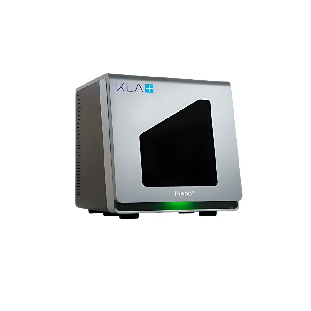
KLA iNano Nanoindentation and Scratch Testing System
| Brand | KLA |
|---|---|
| Origin | USA |
| Model | iNano |
| Load Resolution | <100 nN |
| Displacement Resolution | <0.01 nm |
| Maximum Load Capacity | 500 mN |
| Thermal Drift | <0.05 nm/s (typical) |
| Compliance | ASTM E2546, ISO 14577, ISO 20513, USP <1062>, FDA 21 CFR Part 11 compliant software options available |
Overview
The KLA iNano Nanoindentation and Scratch Testing System is an engineered platform for quantitative nanomechanical characterization of thin films, coatings, bulk materials, and micro-scale specimens. Based on the fundamental principles of quasi-static and dynamic depth-sensing indentation—where a calibrated diamond indenter (typically Berkovich or cube-corner geometry) is driven into the sample surface under controlled force while simultaneously measuring load and displacement with sub-nanometer resolution—the iNano delivers high-fidelity mechanical property data including reduced modulus, hardness, creep compliance, and plasticity index. Its dual-sensor architecture enables simultaneous high-resolution force and displacement feedback across six decades of load range (from <1 µN to 500 mN), making it suitable for heterogeneous material systems—from soft hydrogels and polymer electrolytes to hard ceramic coatings and intermetallic phases. Designed for integration into R&D laboratories, quality control environments, and academic nanomechanics facilities, the iNano operates within a thermally stable, low-vibration enclosure and supports both ambient and environmentally controlled testing conditions.
Key Features
- High-precision electrostatic force actuation and capacitive displacement sensing, delivering <100 nN force resolution and <0.01 nm displacement resolution
- Modular design supporting optional hardware expansions: continuous stiffness measurement (CSM), high-temperature stage (up to 300 °C), in-situ scratch module with lateral force detection, and environmental control chamber
- Integrated motorized XYZ stage with 100 mm × 100 mm travel and 100 nm repeatability for automated multi-point mapping
- Real-time load-displacement curve acquisition at up to 1 kHz sampling rate, enabling transient mechanical response analysis
- Compliance with international standards for nanoindentation testing: ASTM E2546 (Standard Test Method for Instrumented Indentation Hardness), ISO 14577 (Metallic materials — Instrumented indentation test), and ISO 20513 (Hardness testing — Guidelines for the use of instrumented indentation testers)
Sample Compatibility & Compliance
The iNano accommodates planar samples up to 150 mm in diameter and 25 mm in thickness, including polished wafers, cross-sectioned TEM lamellae, sputtered thin-film stacks, and biomedical scaffolds. Surface roughness should be < Ra 10 nm for reliable modulus/hardness quantification; topographic correction algorithms are embedded for moderate roughness compensation. All test protocols support GLP/GMP-aligned documentation workflows when paired with optional audit-trail-enabled software. Data integrity is maintained via time-stamped, digitally signed test records compliant with FDA 21 CFR Part 11 requirements. Optional NanoBlitz™ 3D/4D property mapping modules enable spatially resolved mechanical property reconstruction with voxel resolutions down to 500 nm × 500 nm × 10 nm (lateral × lateral × depth).
Software & Data Management
The iNano is operated through TriboScan™ software—a Windows-based, modular application suite supporting intuitive test setup, real-time visualization, and post-processing analytics. The software includes built-in ISO/ASTM-compliant calculation engines for Oliver–Pharr analysis, CSM-derived storage/loss moduli, scratch adhesion classification (ISO 20502), and statistical reporting across arrays of indentations. Raw data are stored in HDF5 format for long-term archival and third-party interoperability (e.g., MATLAB, Python Pandas). Remote monitoring and video synchronization (via optional integrated microscope camera) allow for correlated morphological and mechanical assessment. Software validation packages—including IQ/OQ documentation, electronic signature configuration, and change control logs—are available for regulated environments.
Applications
- Thin-film mechanical property profiling in semiconductor packaging and MEMS device development
- Hardness and elastic recovery evaluation of PVD/CVD coatings for aerospace and cutting tools
- Nanomechanical mapping of phase-separated polymer blends and battery electrode composites
- Creep and stress relaxation behavior of viscoelastic biomaterials under physiological loading
- Interfacial delamination threshold determination in multilayer optical and barrier coatings via scratch testing
- High-temperature modulus tracking during thermal cycling of solder alloys and interconnect materials
FAQ
What types of indenters are supported by the iNano system?
Standard interchangeable tips include Berkovich, cube-corner, spherical (R = 5 µm, 20 µm), and Vickers geometries—all certified per ISO 14577 Annex B and traceable to NIST standards.
Can the iNano perform tests under inert or humid atmospheres?
Yes—when equipped with the optional environmental chamber, the system supports controlled gas purging (N₂, Ar, forming gas) and relative humidity regulation from 10% to 90% RH at ambient temperature.
Is continuous stiffness measurement (CSM) available as a factory-installed option?
CSM is offered as a standard upgrade path and can be retrofitted to existing iNano systems with firmware and hardware integration verified by KLA Field Applications Engineers.
How does the system ensure measurement reproducibility across different operators and labs?
Through standardized calibration routines (force/displacement), tip geometry certification reports, and SOP-driven test templates—each exportable and version-controlled within TriboScan™ software.
Does the iNano support automated property mapping over large-area samples?
Yes—using the motorized stage and scripting interface (Python API), users can define custom grid patterns, trigger synchronized indentation sequences, and generate 2D/3D mechanical property maps compatible with industry-standard visualization tools.


