LEI-TECH LK-CJS253M Extended Depth-of-Field Digital Microscope with Integrated 3D Metrology
| Brand | LEI-TECH |
|---|---|
| Origin | Tianjin, China |
| Manufacturer Type | Original Equipment Manufacturer (OEM/ODM) |
| Model | LK-CJS253M |
| Price Range | USD $34,000–$41,000 (FOB Tianjin) |
| Optical Interface | Standard C-mount |
| Max Total Magnification | 50×–1000× |
| Sensor | Sony 1/2" CMOS, 2.0 MP (1920 × 1080) |
| Frame Rate | 60 FPS (full HD), 30 FPS (with 3D processing) |
| Shutter | Progressive scan, auto exposure (0.1 ms–16.6 ms), manual range (1 ms–1000 ms) |
| White Balance | Auto / Manual / Region-selectable |
| Video Output | HDMI 2.0 |
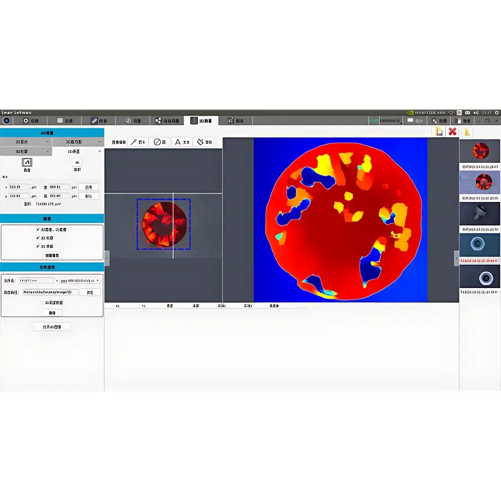
| Core Functions | Real-time Extended Depth of Field (EDF), Wide Dynamic Range (WDR), 3D surface reconstruction, automated 2D/3D metrology, edge-aware segmentation, grayscale gamma correction |
| Measurement Accuracy (10× objective) | ±2 µm (2D & 3D), repeatability ≤2 µm |
| Reporting | Pass/fail classification, batch data export (CSV, PDF, XML), GLP-compliant audit trail (optional software module) |
Overview
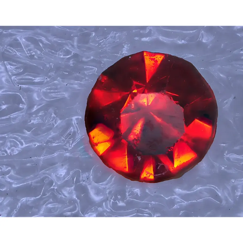
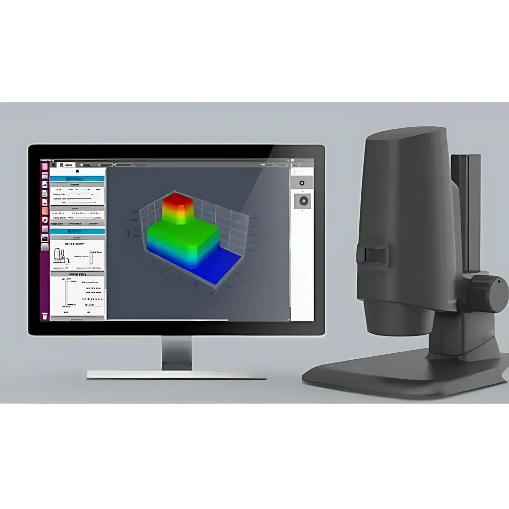
The LEI-TECH LK-CJS253M Extended Depth-of-Field Digital Microscope is an integrated hardware-software solution engineered for high-precision, non-contact 3D surface metrology and extended-focus imaging in industrial quality control, failure analysis, and microstructure characterization environments. Unlike conventional optical microscopes limited by shallow depth of field at high magnifications, the LK-CJS253M employs real-time focus-stacking algorithms combined with synchronized Z-axis motorized stage control (optional) and high-speed CMOS image acquisition to generate artifact-free, fully focused composite images across variable topographies. Its measurement architecture is grounded in photogrammetric triangulation and structured-light-agnostic surface height mapping—enabling traceable dimensional analysis without reliance on interferometric or confocal optics. Designed for seamless integration with reflected-light platforms—including metallurgical, stereo, and monocular microscopes—the system operates as a self-contained imaging node: all core functions are executed onboard, eliminating dependency on external PCs for basic acquisition, rendering, or measurement tasks.
Key Features
- Real-time Extended Depth of Field (EDF): Dynamically fuses sequential focal planes at sub-millisecond intervals, suppressing motion-induced ghosting and maintaining sub-pixel edge fidelity across steep surface gradients.
- Wide Dynamic Range (WDR) Imaging: Compensates for specular reflection from polished metals and ceramics via multi-exposure fusion, preserving texture detail in both highlight and shadow regions without manual gain adjustment.
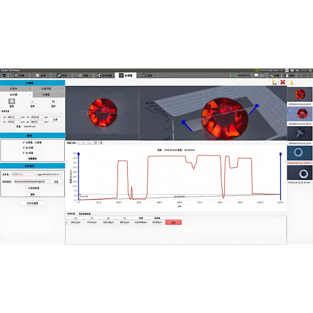
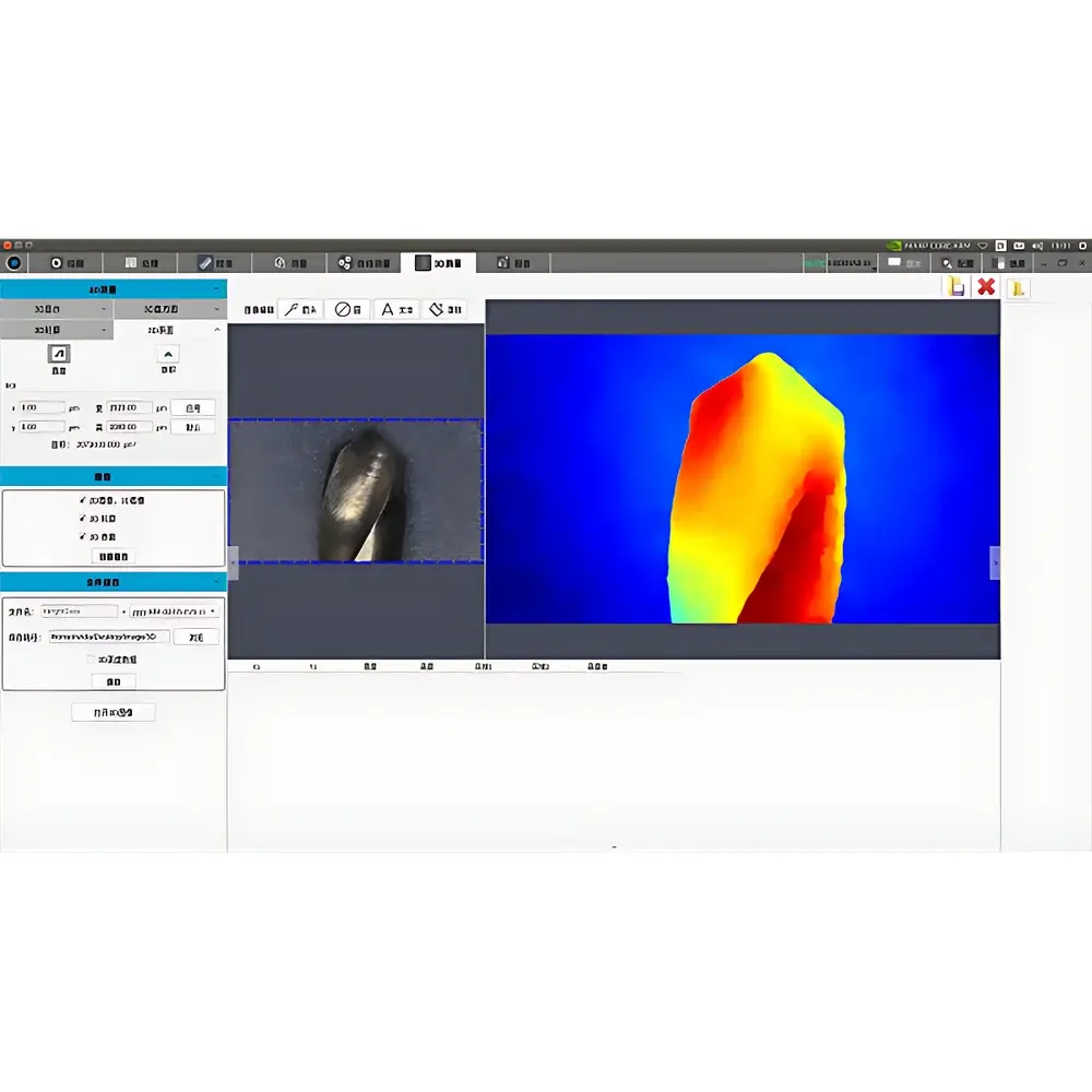
- Onboard 3D Reconstruction Engine: Generates dense point clouds and mesh models directly from Z-stack sequences; supports ISO 25178-compliant surface parameters (Sa, Sq, Sz) when calibrated with NIST-traceable step standards.
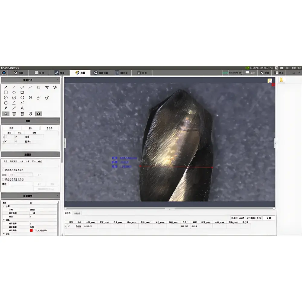
- Automated 2D Metrology Suite: Implements ISO 10360-7–aligned geometric fitting algorithms for circles, parallel lines, polygons, and custom contours—executed with ≤2 µm uncertainty under 10× objective conditions.
- C-mount Interchangeability: Compatible with industry-standard infinity-corrected objectives (5×, 10×, 20×, 50×, 100×) and tube lenses; maintains parfocality and telecentric alignment across magnification changes.
- HDMI 2.0 Real-Time Display: Outputs full-resolution 1080p@60Hz video with embedded measurement overlays, enabling direct monitoring on factory-floor displays or QA station monitors without latency-inducing USB bridges.
Sample Compatibility & Compliance
The LK-CJS253M accommodates reflective, opaque, and semi-transparent specimens common in precision manufacturing: machined metal components (e.g., gear teeth, bearing races), semiconductor wafers, MEMS devices, medical implants, and polymer injection-molded parts. Its EDF/WDR pipeline ensures stable imaging of high-contrast surfaces such as electroplated contacts, anodized aluminum, and sputtered thin films. For regulated environments, optional firmware modules support FDA 21 CFR Part 11 compliance—including electronic signatures, role-based access control, and immutable audit logs for measurement sessions. Calibration certificates per ISO/IEC 17025 are available upon request; system validation documentation aligns with ASTM E2923 (Standard Guide for Measuring and Reporting Microscale Dimensions) and ISO 20967 (Optical 3D imaging systems for industrial applications).
Software & Data Management
The embedded firmware runs LEI-TECH’s proprietary VisionMetro v4.2 platform, featuring dual-mode operation: standalone touchscreen interface (via optional integrated display) and networked remote control (Ethernet/IP). Measurement data—including raw Z-stacks, reconstructed meshes, and annotated 2D profiles—is stored in vendor-neutral HDF5 containers with embedded metadata (timestamp, operator ID, calibration ID, environmental sensor readings). Batch reporting supports automated pass/fail evaluation against user-defined GD&T tolerances (ISO 1101), with exports compliant with ASME Y14.5 and ISO 8015 requirements. Integration with enterprise MES/QMS systems is enabled via RESTful API and OPC UA server mode—supporting SPC charting, statistical process feedback loops, and automated report distribution to SAP QM or Siemens Opcenter modules.
Applications
- Microelectronics: Quantifying solder bump height variation on flip-chip assemblies; measuring trench depth and sidewall angle in etched silicon wafers.
- Precision Machining: Verifying surface roughness and step height on turbine blade cooling holes; assessing burr presence and root radius on threaded fasteners.
- Medical Device QA: Validating coating thickness uniformity on nitinol stents; inspecting laser-weld seam geometry on implant housings.
- Materials Research: Characterizing grain boundary topology in heat-treated alloys; mapping porosity distribution in additively manufactured Ti-6Al-4V lattice structures.
- Forensic & Failure Analysis: Documenting fracture surface morphology in fatigue crack propagation studies; correlating wear scar geometry with tribological test parameters.
FAQ
Does the LK-CJS253M require a dedicated PC for operation?
No—it performs all image acquisition, EDF fusion, 3D reconstruction, and measurement calculations onboard. A PC is optional for advanced data export, network integration, or archival management.
Can the system be calibrated for traceable dimensional measurements?
Yes. Certified calibration kits (NIST-traceable step gauges, grid targets, and sphere arrays) are available. Optional IQ/OQ/PQ documentation packages meet GLP/GMP validation requirements.
What is the maximum working distance achievable with standard objectives?
At 50× magnification, the working distance ranges from 12.5 mm (long-working-distance objective) to 2.1 mm (high-NA metallurgical objective), depending on lens selection.
Is third-party software integration supported?
Yes—via TCP/IP socket protocol and documented JSON-RPC API. MATLAB, Python (OpenCV, PyVista), and LabVIEW drivers are provided under NDA.
How is thermal drift managed during extended 3D acquisitions?
The sensor housing incorporates passive thermal stabilization; internal temperature is monitored continuously, and focus compensation algorithms adjust Z-step increments in real time based on thermal coefficient lookup tables.


