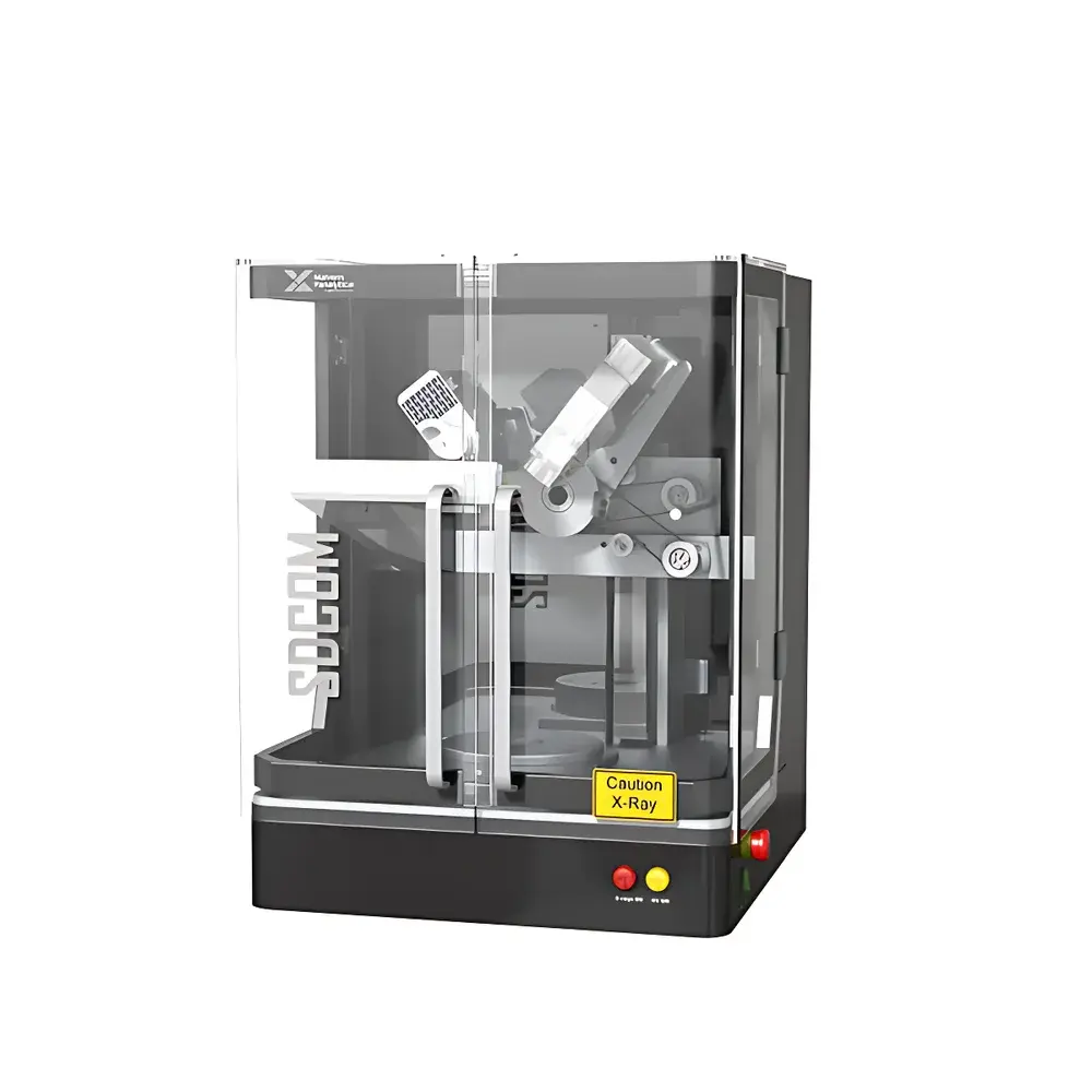
Malvern Panalytical SDCOM Benchtop Single-Crystal X-ray Diffractometer
| Brand | Malvern Panalytical |
|---|---|
| Origin | Netherlands |
| Manufacturer Type | Original Equipment Manufacturer (OEM) |
| Import Status | Imported |
| Model | SDCOM |
| Instrument Type | Single-Crystal X-ray Diffractometer |
| X-ray Source | 30 W air-cooled Cu-anode microfocus X-ray tube |
| Measurement Speed | Full orientation determination in ≤10 s per sample rotation |
| Sample Diameter Range | 1–200 mm |
| Angular Precision (Si 100) | Tilt magnitude < 0.01°, tilt direction < 0.03° |
| Uptime | >99% |
| Theta Scan Capability | Yes |
| Multi-crystal Transfer | Up to 6 oriented crystals per collimated beam |
| MES Integration | Compatible with SECS/GEM-compliant manufacturing execution systems |
Overview
The Malvern Panalytical SDCOM is a compact, benchtop single-crystal X-ray diffractometer engineered for high-precision crystallographic orientation analysis in research laboratories, semiconductor fabrication facilities, and advanced materials production lines. Unlike conventional powder XRD systems, the SDCOM operates on Bragg’s law-based single-crystal diffraction geometry, utilizing monochromatic Cu-Kα radiation (λ = 1.5418 Å) generated by a stable 30 W air-cooled microfocus X-ray tube with a copper anode. Its core function is rapid, non-destructive determination of crystallographic orientation—specifically the Euler angles (φ, θ, ψ)—for bulk single crystals, wafers, and boules. Designed for integration into controlled cleanroom environments, the system delivers industrial-grade repeatability without requiring water cooling, high-voltage infrastructure, or dedicated shielding rooms.
Key Features
- Sub-10-second full orientation measurement cycle per sample rotation—enabled by optimized goniometric kinematics and real-time centroiding algorithms.
- Universal sample stage accommodating diameters from 1 mm (micro-boules) to 200 mm (full-size semiconductor wafers), with motorized Z-height adjustment and vacuum chuck compatibility.
- High angular reproducibility: typical standard deviation of <0.01° in tilt magnitude and <0.03° in tilt direction on Si(100) reference crystals—validated per ISO 17025-accredited internal calibration protocols.
- Robust mechanical architecture featuring thermally stable granite base, direct-drive rotary stages, and backlash-free harmonic drive transmissions for long-term metrological integrity.
- Theta scan mode supporting rocking-curve acquisition (ω-scans), reciprocal space mapping, and lattice parameter refinement for strain and mosaicity assessment.
- Multi-crystal transfer capability: integrated beam-splitting optics allow sequential alignment and indexing of up to six pre-oriented crystals within a single collimated beam path—optimized for high-throughput dicing and epitaxial growth setup.
Sample Compatibility & Compliance
The SDCOM supports quantitative orientation analysis across a broad spectrum of technologically critical single-crystal materials, including but not limited to silicon (Si), silicon carbide (SiC), synthetic diamond, aluminum nitride (AlN), gallium arsenide (GaAs), quartz (α-SiO₂), lithium niobate (LiNbO₃), beta-barium borate (BBO), and gallium nitride (GaN). Its software library includes over 120 pre-parameterized crystal structures with space group symmetry, lattice constants, and reflection lists compliant with the International Tables for Crystallography. The instrument meets CE marking requirements for electromagnetic compatibility (EN 61326-1) and safety (EN 61010-1). Routine operation adheres to ISO 14001 environmental management standards and supports GLP/GMP traceability through audit-ready log files and user-access control tiers.
Software & Data Management
Controlled via Malvern Panalytical’s proprietary CrystalSight™ software suite, the SDCOM provides a deterministic, scriptable workflow environment compliant with FDA 21 CFR Part 11 for electronic records and signatures. All measurements are time-stamped, user-attributed, and stored in vendor-neutral HDF5 format with embedded metadata (sample ID, stage position, exposure parameters, calibration epoch). Batch processing supports automated report generation in PDF/CSV formats, including orientation matrices, pole figures, and misorientation histograms. Native APIs enable bidirectional data exchange with factory-level MES platforms—including SECS/GEM-compliant semiconductor equipment communication standards—ensuring seamless integration into Industry 4.0 digital twin architectures.
Applications
- Semiconductor manufacturing: Pre-epitaxy wafer qualification, off-cut verification, and post-lapping orientation validation for Si, SiC, and GaN substrates.
- Optoelectronics R&D: Precise cut-angle determination for nonlinear optical crystals (e.g., BBO, LBO) used in frequency doubling and parametric oscillation.
- Power electronics: Orientation mapping of SiC boules to identify low-defect sectors prior to wafer slicing.
- Acoustic device fabrication: LiNbO₃ and quartz wafer orientation certification for SAW/BAW filter production.
- Materials science labs: Rapid screening of crystal quality, twinning, and domain structure in ferroelectric and piezoelectric single crystals.
- Quality assurance workflows: Automated pass/fail decision logic based on user-defined angular tolerance bands, exportable to QMS dashboards.
FAQ
What crystallographic information does the SDCOM output?
It reports full Euler angle triplets (φ, θ, ψ), Miller indices of the surface normal and primary reference direction, orientation matrix (g), and angular deviation statistics relative to nominal orientation.
Is the system suitable for measuring strained or mosaic crystals?
Yes—the theta scan function enables rocking curve analysis to quantify full-width-at-half-maximum (FWHM) and assess crystalline perfection, though quantitative strain tensor decomposition requires supplementary reciprocal space mapping.
Does the SDCOM require external cooling or special power conditioning?
No—it operates on standard 100–240 V AC, 50/60 Hz input and uses only air cooling; no chiller, compressed air, or voltage stabilizer is required.
Can it be used for thin-film or polycrystalline samples?
No—the SDCOM is specifically designed for bulk single-crystal characterization; it does not support powder diffraction, grazing-incidence, or texture analysis modes.
How is calibration maintained over time?
The system performs daily self-calibration using an integrated Si(100) reference crystal; all calibrations are logged with NIST-traceable uncertainty budgets and can be re-verified using certified SRM standards.

")