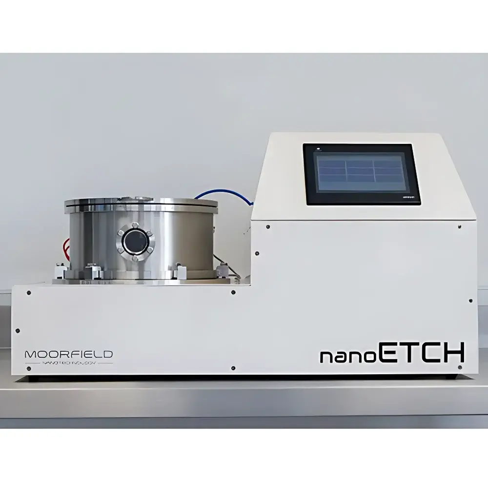
Moorfield nanoETCH Desktop Ultra-Precision Plasma Soft Etching System for 2D Materials
| Brand | Moorfield |
|---|---|
| Origin | United Kingdom |
| Model | nanoETCH |
| RF Power Range | <30 W (milliwatt-resolution control) |
| Base Pressure | <5×10⁻⁷ mbar |
| Sample Stage Options | 3-inch & 6-inch |
| Vacuum System | Turbomolecular pump with optional backing pump |
| Gas Delivery | Mass Flow Controller (MFC)-regulated |
| Control Interface | Integrated touchscreen HMI with programmable etch recipes |
| Data Logging | PC-compatible USB/Ethernet interface |
| Safety Compliance | CE, IEC 61000-6-4, IEC 61000-6-2 |
Overview
The Moorfield nanoETCH is a purpose-built desktop plasma soft etching system engineered specifically for the atomic-scale processing of van der Waals heterostructures and monolayer two-dimensional (2D) materials—including graphene, transition metal dichalcogenides (TMDs), hexagonal boron nitride (h-BN), and black phosphorus. Unlike conventional reactive ion etching (RIE) or inductively coupled plasma (ICP) systems designed for silicon-based semiconductor fabrication, the nanoETCH employs a low-energy, capacitively coupled plasma (CCP) architecture with milliwatt-level RF power resolution. This enables sub-monolayer material removal—critical for preserving the intrinsic electronic, optical, and mechanical properties of atomically thin films. The system operates under ultra-high vacuum (UHV) conditions (<5×10⁻⁷ mbar), minimizing hydrocarbon contamination and enabling reproducible surface chemistry control. Its compact footprint, integrated turbomolecular pumping, and fully enclosed RF chamber meet stringent cleanroom Class 100–Class 10 requirements, making it suitable for integration into academic nanofabrication facilities, national research centers, and industrial R&D labs focused on next-generation quantum and flexible electronics.
Key Features
- Milliwatt-resolution RF power control (<30 W range) for layer-by-layer and defect-selective etching of 2D materials
- UHV-compatible chamber with base pressure <5×10⁻⁷ mbar, achieved via oil-free turbomolecular pumping
- Programmable multi-step etch recipes stored and executed via intuitive touchscreen HMI
- Dual-stage sample platforms supporting 3-inch and 6-inch wafers or custom substrates (e.g., SiO₂/Si, quartz, sapphire)
- Precise gas dosing using calibrated mass flow controllers (MFCs) for Ar, O₂, CHF₃, SF₆, N₂, and custom gas mixtures
- Real-time process monitoring with integrated RF forward/reflected power metering and pressure feedback
- Fully traceable data logging via USB or Ethernet to external PCs; compatible with LabVIEW and Python-based automation
- CE-marked enclosure with interlocked access doors, emergency stop circuitry, and RF shielding per IEC 61000-6-4
- Modular design enabling field-upgradable options: ultra-stable RF generator (<±0.1% power stability), high-precision pressure regulation (<0.01 mbar resolution), and rapid chamber venting
Sample Compatibility & Compliance
The nanoETCH supports direct processing of exfoliated, CVD-grown, or transferred 2D materials on insulating, semiconducting, or metallic substrates—including SiO₂/Si, Al₂O₃, h-BN, PET, and flexible polyimide. It has been validated for use in GLP-aligned research environments and meets essential electromagnetic compatibility (EMC) and safety standards: IEC 61000-6-2 (immunity), IEC 61000-6-4 (emissions), and EN 61010-1 (electrical safety). While not certified for GMP production, its audit-ready operation log, recipe versioning, and user-access-level permissions align with pre-production R&D workflows requiring traceability per ISO/IEC 17025 and ASTM E2500-21 guidelines. All internal wetted surfaces are electropolished stainless steel or anodized aluminum, ensuring minimal outgassing and compatibility with oxygen plasma cleaning protocols required prior to 2D material transfer.
Software & Data Management
The nanoETCH runs on a real-time Linux-based embedded OS with a responsive 10.1″ capacitive touchscreen interface. Users define etch parameters—including RF power ramp profiles, gas composition sequences, pressure setpoints, and duration per step—via drag-and-drop recipe builder. Each executed run generates a timestamped .csv file containing RF power, chamber pressure, gas flows, and system status flags. Optional software modules support remote monitoring via web browser (HTTPS), automated report generation (PDF/HTML), and integration with LIMS or ELN platforms through RESTful API endpoints. Audit trails include operator ID, recipe name/version, start/stop timestamps, and checksum-verified raw data—fully compliant with FDA 21 CFR Part 11 requirements when deployed with enterprise authentication and digital signature add-ons.
Applications
- Sub-monolayer etching of graphene for Hall bar, QPC, and nanoribbon device patterning
- Controlled defect engineering: creation of vacancy clusters, line defects, or dopant-selective sites for sensing applications
- Surface functionalization of graphite and h-BN substrates to modulate van der Waals epitaxy
- Pre-transfer substrate cleaning to eliminate organic residues without damaging native oxide layers
- Edge passivation of TMD flakes via low-dose O₂ plasma exposure
- Integration with dry transfer stations for in-situ cleaning and edge trimming prior to heterostructure assembly
- Development of pyroelectric bolometers, Dirac billiards, and vertical heterojunction FETs—as demonstrated in peer-reviewed studies published in Nature Materials, Science, and Nature Nanotechnology
FAQ
What distinguishes nanoETCH from standard RIE systems?
Unlike high-power RIE tools optimized for Si or GaN, nanoETCH uses milliwatt-resolved CCP plasma to avoid lattice damage, ion bombardment-induced disorder, and unintended doping—enabling true atomic-layer precision on fragile 2D crystals.
Can nanoETCH process suspended membranes or freestanding flakes?
Yes—its low-ion-energy regime (<5 eV average ion energy) and uniform plasma distribution minimize mechanical stress, allowing direct etching of suspended graphene or MoS₂ over microcavities.
Is the system compatible with glovebox integration?
Absolutely—the nanoETCH features standardized KF-40 vacuum flanges and optional inert-gas purge ports, enabling seamless coupling to nitrogen- or argon-purged gloveboxes for air-sensitive 2D material handling.
What maintenance is required for long-term UHV performance?
Annual turbomolecular pump bearing inspection and quarterly MFC recalibration are recommended; all consumables—including RF matching network capacitors and ceramic chamber liners—are field-replaceable with no alignment tools.
Does Moorfield provide application support for new 2D material systems?
Yes—Moorfield’s Applications Lab offers remote process optimization, method development reports, and co-authored publication support for academic users, backed by direct collaboration with the University of Manchester’s National Graphene Institute.


