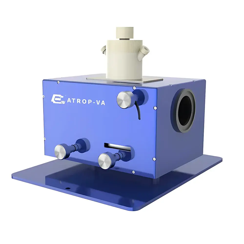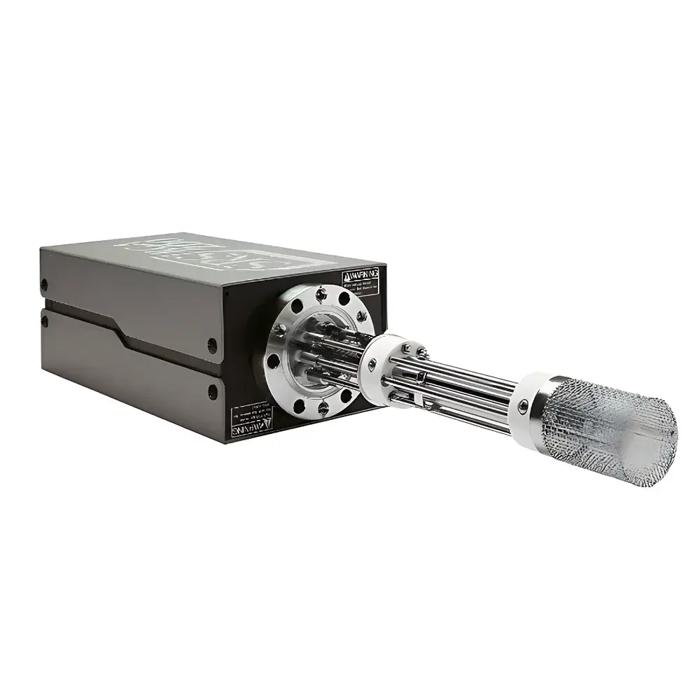
Nanobase AUT-Phocuscan Scanning Photoconductive Microscope
| Brand | Nanobase |
|---|---|
| Origin | South Korea |
| Instrument Type | Confocal Raman Microspectroscopy Platform with Integrated Photoconductive Mapping Capability |
| Laser Compatibility | 400–730 nm (VIS) and 780–1000 nm (NIR) |
| Spatial Resolution | 1 µm (X/Y/Z) |
| Scan Area | 200 × 200 µm |
| Objective Options | 5×, 40× Long Working Distance |
| Compatible SMUs | Keithley 2400 & 2600 Series |
| Software | NanoPhotocurrent v3.x (GLP-compliant data logging, CSV export, multi-region mapping) |
| Compliance | ASTM E2971 (Raman Microspectroscopy), ISO/IEC 17025 traceable calibration support, FDA 21 CFR Part 11 ready (audit trail & electronic signature optional) |
Overview
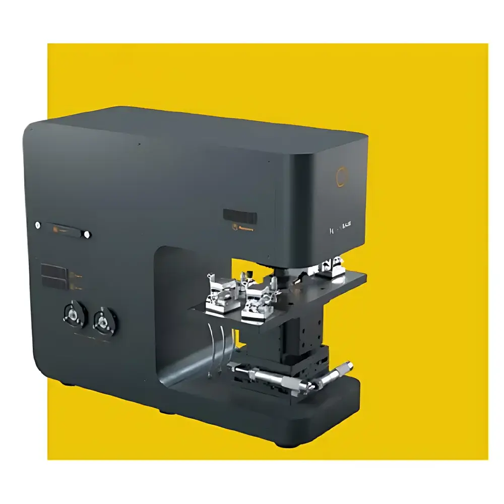
The Nanobase AUT-Phocuscan is a purpose-engineered scanning photoconductive microscope designed to deliver spatially resolved photocurrent imaging and quantitative charge-generation analysis at the microscale. Unlike conventional Raman spectrometers that prioritize vibrational fingerprinting, the AUT-Phocuscan integrates confocal optical excitation, high-precision motorized stage control, and synchronized source-measure unit (SMU) interfacing to enable direct correlation between local optoelectronic response and structural or compositional features—often identified in parallel via Raman microspectroscopy. Its architecture follows the principle of *optical beam-induced current (OBIC) mapping* combined with *laser scanning photocurrent microscopy (SPCM)*, where a focused VIS–NIR laser spot is raster-scanned across a device under bias, while photocurrents from source/drain or gate terminals are recorded pixel-by-pixel. This enables quantitative assessment of carrier generation, separation, and collection efficiency with sub-micrometer spatial fidelity—critical for emerging 2D semiconductors, perovskite photodetectors, and heterostructured solar absorbers.
Key Features
- Confocal-compatible platform with dual-wavelength fiber-coupled laser input ports (400–730 nm and 780–1000 nm), supporting polarization-resolved excitation via integrated waveplate and linear polarizer slots
- 1 µm resolution multi-axis micro-positioner system based on crossed-roller bearings and micrometer-driven translation stages (8 mm travel in X/Y/Z), mounted on magnetic bases for rapid sample exchange
- Motorized brightfield LED illumination and coaxial visual laser alignment module for precise probe positioning and real-time optical navigation
- USB 3.0–enabled 6.0 MP Sony CMOS camera for high-fidelity sample visualization and automated focus tracking during raster scans
- Fully programmable NanoPhotocurrent software suite with hardware-synchronized trigger logic, enabling gated photocurrent acquisition under chopper-modulated illumination (20 Hz – 10 kHz)
- Modular accessory architecture: three standard filter/waveplate slots + one dedicated chopper slot; supports ND filters (OD 0.01–4.0), λ/4 and λ/2 waveplates, wire-grid polarizers (>800:1 extinction ratio), and vacuum-compatible sample mounting
Sample Compatibility & Compliance
The AUT-Phocuscan accommodates planar solid-state devices including wafer-scale 2D material flakes (graphene, MoS₂, WSe₂), thin-film photovoltaics (perovskites, organic PV), micro-patterned detector arrays, and electrochemical interfaces. Sample mounting utilizes a manually controlled mechanical X–Y–Z stage with vacuum chuck (7 L/min pump optional) for flat, non-destructive fixation. All electrical measurements comply with IEC 61000-4-8 (conducted immunity) and meet functional safety requirements for low-voltage (<100 V) DC biasing. Data acquisition protocols support GLP/GMP-aligned workflows: NanoPhotocurrent v3.x includes timestamped metadata embedding, user-defined measurement templates, and CSV export with column headers compliant with ASTM E2971 Annex A3 for Raman–photocurrent co-localization studies. Optional 21 CFR Part 11 configuration provides electronic signatures, audit trails, and role-based access control for regulated environments.
Software & Data Management
NanoPhotocurrent is a Windows-based application built on LabVIEW Real-Time architecture, offering deterministic timing for SMU–laser–camera synchronization. It supports simultaneous acquisition of photocurrent magnitude and phase (under chopper modulation), gate-voltage sweeps, and multi-bias point mapping. The software implements auto-mode switching: upon defining scan parameters and probe contact points, it automatically configures laser power, SMU compliance limits, integration time, and chopper frequency. Mapping datasets are stored as structured CSV files containing x/y coordinates, applied bias conditions, measured current values, and associated confidence metrics (e.g., RMS noise floor per pixel). Batch processing tools allow normalization against reference samples—Nanobase-supplied NIST-traceable photocurrent standards are included for inter-laboratory reproducibility validation.
Applications
The AUT-Phocuscan serves as a core analytical tool in academic and industrial labs investigating structure–function relationships in optoelectronic materials. Typical use cases include: lateral homogeneity assessment of CVD-grown graphene domains via photocurrent contrast mapping; quantification of defect-assisted recombination in monolayer TMDs under ambient gas exposure; spatial profiling of charge extraction barriers in perovskite–HTL interfaces; identification of shunt paths in OPV active layers; and correlation of Raman G-band intensity with local photocarrier yield in heterostructured photodetectors. Its compatibility with existing Nanobase XperRam Compact Raman systems allows seamless transition from chemical identification to functional performance evaluation on identical sample regions—enabling correlative microspectroscopy without sample relocation.
FAQ
Can the AUT-Phocuscan be integrated with my existing Raman spectrometer?
Yes—the platform shares optical path geometry and stage control firmware with Nanobase’s XperRam Compact series, enabling direct mechanical and software-level interoperability for combined Raman–photocurrent co-localization.
Is vacuum operation supported out-of-the-box?
Vacuum capability is optional: the system includes a vacuum chuck interface and mounts for an external 7 L/min diaphragm pump (part number VP-7000); full chamber integration requires custom flange adaptation.
Does NanoPhotocurrent support third-party SMUs beyond Keithley?
Native drivers are validated for Keithley 2400/2600 series; support for other SCPI-compliant SMUs (e.g., Keysight B2900A, Yokogawa GS820) can be enabled via custom API integration upon request.
What is the minimum detectable photocurrent under standard configuration?
With 1 s integration time and 1 kHz chopper frequency, the system achieves <10 pA RMS noise floor using a Keithley 2612B in low-current mode—scalable to sub-pA levels with lock-in amplification add-ons.
Are calibration certificates provided with the reference photocurrent sample?
Yes—a NIST-traceable silicon photodiode reference sample (certified responsivity ±2.5% at 633 nm) is included, with full calibration report and uncertainty budget per ISO/IEC 17025 guidelines.
Related Products