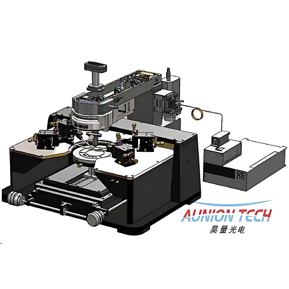
Nanobase PL_Mapping_System Confocal Raman-Photocurrent Imaging System
| Brand | Nanobase |
|---|---|
| Origin | South Korea |
| Model | PL_Mapping_System |
| Instrument Type | Confocal Micro-Raman Spectrometer with Integrated Photocurrent Mapping Capability |
| Spectral Range | 30–6000 cm⁻¹ |
| Spectral Resolution | < 0.02 µm (equivalent to < 0.5 cm⁻¹ at 532 nm) |
| Spatial Resolution | < 0.02 µm (diffraction-limited, dependent on objective NA and excitation wavelength) |
| Spectral Reproducibility | < 0.1 µm (wavelength stability over time and position) |
| Excitation Wavelengths | 445, 532, 635, 808, 1530 nm |
| Field of View | 200 µm × 200 µm (with 40×, NA = 0.75 objective) |
| XY Stage Travel | 150 mm × 150 mm (5 µm resolution) |
| Z-Travel | ±10 mm (1 µm resolution) |
| Probe Station | 6-inch vacuum chuck, gold/tungsten probes, PH-C15 high-precision manipulators, leakage current < 10 fA |
Overview
The Nanobase PL_Mapping_System is a fully integrated confocal micro-spectroscopic imaging platform engineered for simultaneous Raman spectroscopy, photoluminescence (PL), electroluminescence (EL), and spatially resolved photocurrent mapping. It combines a high-stability laser scanning microscope with a cryo-compatible probe station and a volume-phase holographic grating (VPHG) spectrometer—enabling quantitative, correlative optical and electronic characterization at sub-diffraction spatial scales. The system operates on the principle of point-by-point confocal excitation and spectral detection: a focused laser beam raster-scans the sample surface while collecting backscattered Raman photons, emitted PL/EL photons, or generated photocurrents via integrated microprobes. This architecture supports true multimodal hyperspectral imaging—where each pixel contains a full Raman spectrum (30–6000 cm⁻¹), a PL emission profile, and a bias-dependent photocurrent response—all co-registered with nanoscale positional fidelity.
Key Features
- Confocal laser scanning architecture with < 0.02 µm lateral resolution (at 532 nm, NA = 0.75), enabling sub-wavelength optical sectioning and depth-resolved analysis.
- VPHG spectrometer with >90% diffraction efficiency across visible and NIR bands—delivering superior signal throughput compared to reflective grating systems.
- Modular probe station with 6-inch vacuum chuck, motorized XYZ stage (150 × 150 × ±10 mm travel), and low-leakage (<10 fA) tungsten/gold probes for in situ electrical stimulation and current measurement.
- Multi-wavelength excitation support (445, 532, 635, 808, 1530 nm) with automated filter switching—optimized for resonance Raman, defect-sensitive PL, and bandgap-tuned photocurrent generation.
- High-speed 2D mapping capability over 200 µm × 200 µm fields-of-view at frame rates up to 100 spectra/sec per pixel (dependent on integration time and spectral binning).
- Fully customizable optical path—supports future upgrades including time-resolved PL, polarization-resolved Raman, and cryogenic operation down to 4 K (with optional cryostat integration).
Sample Compatibility & Compliance
The PL_Mapping_System accommodates rigid and flexible substrates—including Si/SiO₂ wafers, TEM grids, glass slides, polymer films, and freestanding 2D materials—without requiring metallization or conductive coatings. Its non-contact optical excitation and low-noise current amplification (fA-level sensitivity) ensure minimal sample perturbation during measurement. The system meets essential laboratory compliance requirements for research-grade instrumentation: mechanical design conforms to ISO 14644-1 Class 5 cleanroom compatibility; electrical safety complies with IEC 61010-1; and data acquisition protocols support audit-ready metadata logging aligned with GLP principles. While not certified for clinical diagnostics, its measurement traceability is compatible with ASTM E1840 (Raman spectral calibration) and ISO/IEC 17025 documentation practices for accredited testing laboratories.
Software & Data Management
Control and analysis are executed via Nanobase’s proprietary XperRam software suite—a modular, scriptable platform built on LabVIEW and Python APIs. It provides real-time spectral preview, automated background subtraction, multivariate curve resolution (MCR), peak fitting (Voigt/Gaussian deconvolution), and spatial correlation matrices between Raman shifts, PL intensity, and photocurrent magnitude. All raw hyperspectral cubes (Raman + PL + Iphoto) are saved in HDF5 format with embedded metadata (laser power, objective ID, stage coordinates, bias voltage, temperature). The software supports export to common formats (CSV, TIFF, .spc) and integrates with third-party tools such as MATLAB, OriginPro, and HyperSpy for advanced statistical modeling. Audit trails—including user login timestamps, parameter changes, and data export events—are retained for ≥18 months, satisfying internal QA requirements and preliminary alignment with FDA 21 CFR Part 11 electronic record controls.
Applications
This system is routinely deployed in academic and industrial R&D labs for structure–property–function correlation in emerging functional materials. In 2D material science, it maps strain distribution (via Raman G-band shift), layer stacking order (2D-mode splitting), defect density (D/G ratio), and local photoresponse heterogeneity (photocurrent quantum yield) across graphene, MoS₂, and h-BN flakes. In perovskite and organic photovoltaics, it identifies phase segregation (PL spectral clustering), ion migration pathways (bias-dependent Raman mode evolution), and electrode–active-layer interfacial recombination (spatially resolved EL quenching). In ferroelectric oxides, it correlates domain wall conductivity (nanoscale photocurrent spikes) with phonon softening (Raman frequency collapse near TC). Additional use cases include single-cell optoelectronic phenotyping, OLED emissive layer uniformity assessment, and catalytic surface reaction monitoring under operando illumination.
FAQ
What excitation wavelengths are standard, and can custom lasers be integrated?
Standard configurations include 445, 532, 635, 808, and 1530 nm diode lasers. OEM laser modules (e.g., pulsed UV or OPO-tuned sources) may be integrated via fiber-coupled ports with prior optical path recalibration.
Is cryogenic operation supported out-of-the-box?
The base system is compatible with external cryostats (e.g., Janis ST-500, Montana Instruments CryoMS). Vacuum feedthroughs and thermal anchoring provisions are included; full low-temperature Raman/photocurrent correlation requires optional cold-stage alignment kits.
How is photocurrent quantified, and what is the minimum detectable current?
Photocurrent is measured using a calibrated transimpedance amplifier with selectable gain (10⁶–10¹¹ V/A). The system achieves 10 fA RMS noise floor (1 Hz bandwidth), enabling reliable detection of sub-picoamp responses from micron-scale devices.
Can Raman, PL, and photocurrent data be acquired simultaneously?
Yes—time-synchronized acquisition is enabled via hardware triggering. Each pixel records a full Raman spectrum, integrated PL intensity, and averaged photocurrent under identical illumination and bias conditions.
What level of technical support and application assistance is provided?
Nanobase offers remote commissioning, on-site training (2 days), and annual application workshops. Local distributor engineering support includes preventive maintenance, spectral calibration verification, and method development for novel material systems.