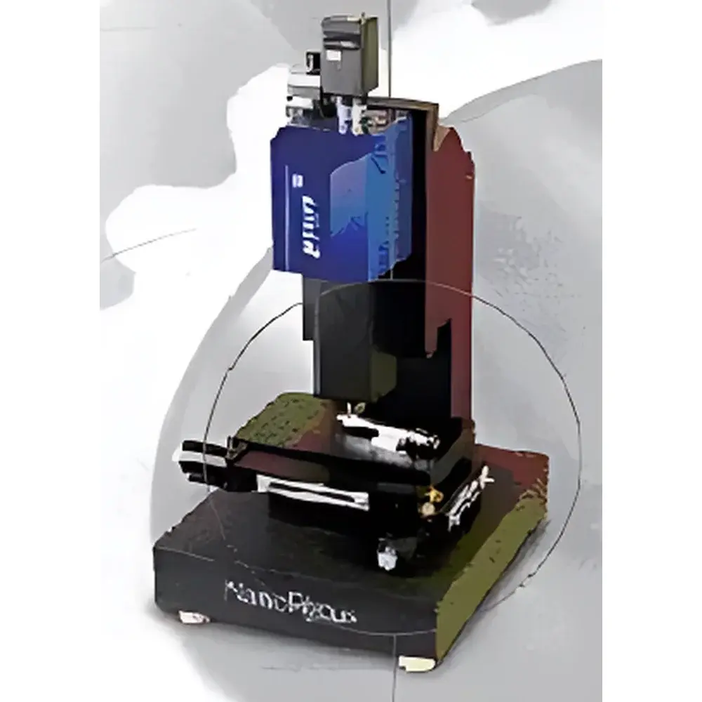
Nanofocus μSurf White-Light Confocal Profilometer
| Origin | Germany |
|---|---|
| Manufacturer Type | Authorized Distributor |
| Origin Category | Imported |
| Model | Nanofocus μSurf |
| Pricing | Upon Request |
Overview
The Nanofocus μSurf White-Light Confocal Profilometer is a high-precision, non-contact surface metrology instrument engineered for sub-nanometer vertical resolution and micron-level lateral accuracy in 3D topographic characterization. It operates on the principle of white-light confocal microscopy: a broadband halogen or xenon light source is focused through a high-numerical-aperture (NA) objective onto the sample surface; only the in-focus plane produces maximum intensity at the pinhole-detected photodetector. Vertical scanning (z-axis) enables precise determination of peak intensity position per lateral (x,y) pixel—yielding true height data with exceptional axial discrimination and minimal chromatic aberration artifacts. Designed for ISO 25178-compliant areal surface texture analysis, the μSurf delivers traceable, repeatable measurements across microstructured surfaces, MEMS devices, optical components, medical implants, and precision-machined parts—without sample coating or vacuum requirements.
Key Features
- Modular confocal measurement head with interchangeable optical modules (1600 S, 800 L/S/XS, 320 L/S/XS, 160 L/S) supporting NA values from 0.3 to 0.95 and working distances ranging from 0.3 mm to 12 mm—enabling optimal trade-offs between resolution, field-of-view, and accessibility.
- High-speed digital imaging: dual-camera options—BM 512 (512 × 512, 8-bit, up to 25 fps) or fast-firewire camera (512 × 512, 12-bit, up to 58 fps)—ensuring robust signal-to-noise ratio and efficient data acquisition for dynamic or large-area scans.
- Precision motion control: motorized XY stage (50 × 50 mm travel, 0.1 µm encoder resolution) combined with either ZM 100 (100 mm range, 0.1 µm resolution) or NV 350 piezo scanner (350 µm range, <1 nm resolution, sub-2 nm noise floor) for ultra-stable, vibration-insensitive vertical profiling.
- Adjustable illumination: selectable halogen (LS 100) or high-intensity xenon (LX 100/LX 180) light sources—optimized for reflectivity contrast across metallic, dielectric, and transparent substrates.
- Rugged industrial-grade architecture with thermal stabilization and active drift compensation—designed for integration into cleanroom environments and production-line QA labs under GLP/GMP conditions.
Sample Compatibility & Compliance
The μSurf accommodates samples from 10 mm × 10 mm up to 200 mm × 200 mm (with optional extended stage), including curved, tilted, or multi-material surfaces. Its non-destructive, ambient-air operation eliminates charging artifacts common in SEM-based profiling and avoids UV-induced degradation of polymers or photoresists. All measurement protocols comply with ISO 25178-2 (areal surface texture parameters), ISO 4287/4288 (profile-based roughness), and ASTM E2927-19 (standard guide for confocal microscopy in surface metrology). Data integrity meets FDA 21 CFR Part 11 requirements when used with validated software configurations—including electronic signatures, audit trails, and secure user access controls.
Software & Data Management
Controlled via μSoft®—a dedicated Windows-based platform supporting real-time scan preview, automated focus search, multi-region stitching, and batch processing. The software provides full ISO 25178 parameter sets (Sa, Sq, Sz, Ssk, Sku, etc.), filtering (Gaussian, spline, robust), and advanced analysis modules for step-height, curvature, volume, and bearing ratio (Abbott-Firestone curve). Raw data export supports ASCII, CSV, and standard .sur/.xyz formats; integration with MATLAB, Python (via API), and metrology databases (e.g., Q-DAS, Siemens Teamcenter) is fully supported. Audit logs record operator ID, timestamp, instrument configuration, calibration status, and raw image metadata—ensuring full traceability for ISO 17025-accredited laboratories.
Applications
- Characterization of micro-optics (lens arrays, diffractive elements, AR coatings) requiring <5 nm z-resolution and sub-µm lateral fidelity.
- Quantitative assessment of machined surface integrity—tool marks, burrs, waviness—in aerospace turbine blades and orthopedic implant substrates.
- 3D inspection of semiconductor packaging features (solder bumps, redistribution layers, TSVs) and MEMS cantilevers with aspect ratios >10:1.
- Quality control of injection-molded polymer optics, including demolding defect mapping and replication fidelity analysis against master tools.
- Research-grade topography of graphene transfer layers, thin-film solar cells, and battery electrode coatings—where non-contact, ambient-condition measurement is critical.
FAQ
What is the smallest measurable feature size in lateral (x,y) direction?
Lateral resolution depends on optical module selection: down to 0.31 µm with the 160 XS objective (NA = 0.95), verified per ISO 10110-7 using calibrated line-width standards.
Can the system measure transparent or highly reflective surfaces?
Yes—via optimized xenon illumination (LX series), polarization control, and adaptive exposure algorithms that suppress glare and internal reflections without neutral-density filters.
Is the NV 350 piezo scanner compatible with all optical modules?
The NV 350 is designed for high-resolution applications and pairs exclusively with objectives offering NA ≥ 0.5; it is not recommended with long-working-distance (L-type) modules due to mechanical coupling constraints.
Does the system support automated calibration verification?
Yes—μSoft includes built-in routines for daily performance checks using NIST-traceable step-height and roughness reference artifacts (e.g., VDI/VDE 2634 Class 1 standards).
How is thermal drift compensated during long-duration scans?
The μSurf incorporates an integrated temperature sensor array and real-time z-position correction algorithm, reducing thermal drift to <10 nm over 2-hour continuous operation at ±0.5 °C ambient stability.