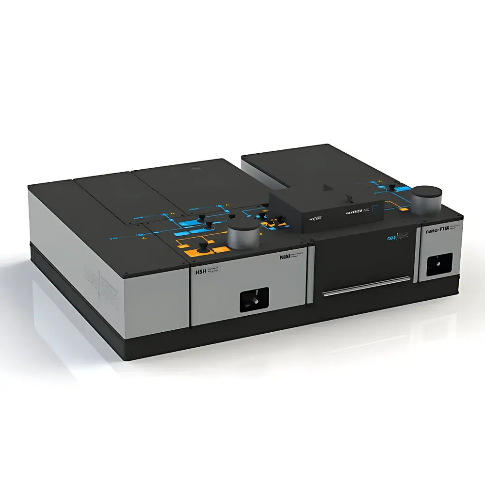
Neaspec nano-FTIR o-FTIR Scattering-type Near-field Fourier Transform Infrared Spectrometer
| Brand | Neaspec |
|---|---|
| Origin | Germany |
| Model | o-FTIR |
| Instrument Type | Laboratory-based FTIR Spectrometer |
| Spatial Resolution | 10 nm |
| Spectral Resolution | 3.0 cm⁻¹ |
| Acquisition Speed | 3 spectra/s |
| Signal-to-Noise Ratio | 80:1 |
| Spectral Range | 0.5–20 µm (Visible to Mid-IR) |
| Illumination Mode | Reflection-mode AFM tip illumination |
| Detection | Interferometric scattering near-field detection with background-free architecture |
Overview
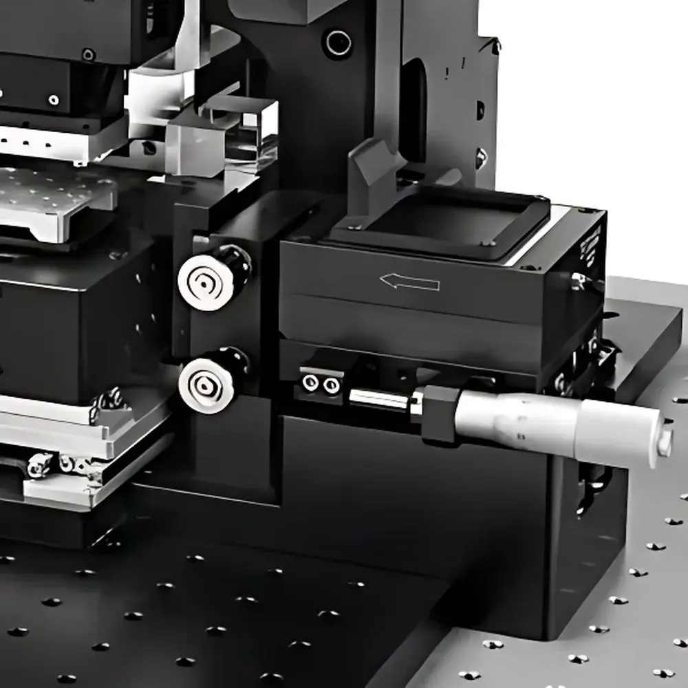
The Neaspec nano-FTIR o-FTIR is a laboratory-grade scattering-type near-field Fourier transform infrared spectrometer engineered for nanoscale chemical identification without physical contact or sample destruction. Unlike conventional FTIR spectroscopy—limited by the diffraction barrier (~λ/2, typically >3–10 µm in mid-IR)—this instrument overcomes the resolution limit via scattering-type scanning near-field optical microscopy (s-SNOM). It combines atomic force microscopy (AFM) topographic precision with broadband interferometric infrared detection to deliver true nanoscale vibrational spectroscopy. The system operates on the principle of coherent heterodyne detection: an infrared laser illuminates a sharp metallic AFM tip, generating localized near-field enhancement at the tip apex; scattered light containing both amplitude and phase information is interferometrically recorded and Fourier-transformed to yield absorption spectra. Critically, nano-FTIR spectra exhibit direct spectral correspondence with far-field FTIR reference databases—enabling unambiguous molecular fingerprint matching without empirical modeling or Kramers–Kronig transformation.
Key Features
- 10 nm spatial resolution: Achieved through s-SNOM with λ/1000 localization, enabling spectroscopic mapping of single-molecule monolayers, 2D materials, and sub-10 nm contaminants.
- True FTIR spectral fidelity: Near-field absorption spectra match standard FTIR library references (e.g., NIST, Sadtler) with no baseline correction or dispersion modeling required.
- Background-free interferometric detection: Patented dual-channel interferometry suppresses far-field background, ensuring high dynamic range and quantitative linearity.
- Multi-spectral acquisition: Up to 3 full interferograms per second, compatible with lock-in demodulation orders n = 1–4 for optimized signal-to-noise trade-off.
- Broadband spectral coverage: Configurable beam path supports visible (0.5 µm), near-IR, and mid-IR (up to 20 µm) using exchangeable beamsplitters and detectors.
- Non-contact, non-destructive operation: Pure optical detection mechanism—no thermal expansion dependency—ideal for low-thermal-expansion materials (graphene, h-BN, oxides, ultrathin polymers).
Sample Compatibility & Compliance
The nano-FTIR o-FTIR accommodates conductive and insulating samples—including 2D materials, polymer blends, biological membranes, catalytic nanoparticles, and semiconductor heterostructures—without metallization or sectioning. Its reflection-mode tip illumination enables analysis of opaque, rough, or buried interfaces (e.g., electrode/electrolyte, Si/SiO₂, metal/organic monolayers). The system meets essential regulatory frameworks for research integrity: data acquisition logs include timestamped metadata (laser power, scan position, interferometer path difference, detector gain), supporting GLP-compliant documentation. While not certified for GMP production environments, its audit-trail-ready software architecture aligns with FDA 21 CFR Part 11 principles for electronic records in academic and industrial R&D labs. All optical components comply with ISO 10110 surface quality standards; mechanical stages conform to ISO 9283 repeatability specifications (±2 nm typical).
Software & Data Management
Control and analysis are performed via Neaspec’s proprietary NanoDrive™ software suite, built on a modular LabVIEW-based architecture. Core modules include real-time interferogram acquisition, phase-resolved near-field spectrum reconstruction, hyperspectral image stitching, and multivariate spectral decomposition (PCA, cluster analysis). Spectra are exported in standardized formats (JCAMP-DX, HDF5, ASCII) for interoperability with commercial chemometrics platforms (GRAMS/AI, OPUS, Python SciPy). The software enforces version-controlled experiment templates, user-access permissions, and encrypted project archives. Raw interferograms retain full phase information—enabling post-acquisition reprocessing for advanced applications such as plasmon dispersion mapping or phonon-polariton dispersion analysis. Automated calibration routines reference NIST-traceable CO₂ and H₂O vapor lines for spectral axis validation.
Applications
- 2D material chemistry: Identification of covalent vs. non-covalent functionalization on graphene, MoS₂, and hexagonal boron nitride at monolayer resolution—validated in Nature Chemistry (2021) for fantrip photopolymerization kinetics.
- Electrochemical interfaces: In situ nanoscale probing of electric double layers on graphene electrodes under potentiostatic control—revealing voltage-dependent ion coordination signatures undetectable by ATR-FTIR (Nano Letters, 2019).
- Polymer nanocomposites: Chemical mapping of PS/PMMA/PVDF blends with 30 nm spatial resolution and peak-specific distribution imaging (C–F, C=O, C–O bands), published in Nature Communications (2017).
- Contaminant forensics: Unambiguous identification of sub-100 nm PDMS particles at Si/PMMA interfaces via spectral library matching—eliminating ambiguity from topographic or phase contrast alone.
- Quantum material phononics: Mapping of hyperbolic phonon polaritons in α-MoO₃ and reststrahlen band engineering in vanadium dioxide phase transitions (Nature Nanotechnology, Science).
FAQ
How does nano-FTIR differ from AFM-IR or photothermal IR microspectroscopy?
nano-FTIR uses interferometric s-SNOM with phase-sensitive detection, delivering true absorption spectra without thermal artifacts. AFM-IR relies on photothermal expansion, limiting sensitivity on low-expansion materials; photothermal methods lack phase information and suffer from thermal diffusion blurring.
Can nano-FTIR be coupled to synchrotron IR sources?
Yes—the instrument includes a dedicated port for external broadband IR beam injection and supports vacuum-compatible optics for synchrotron integration, as demonstrated at BESSY II and ALS.
Is spectral quantification possible?
Quantitative absorption cross-sections are accessible via calibrated reference measurements on isotopically enriched standards or thin-film thickness metrology (e.g., ellipsometry), though absolute extinction coefficients require careful near-field correction modeling.
What sample preparation is required?
None beyond standard clean-room handling. No coating, embedding, or sectioning is needed. Samples must be mounted on flat, non-reflective substrates (e.g., CaF₂, Si wafers) compatible with AFM scanning.
Does the system support time-resolved measurements?
While not designed for ultrafast pump-probe, it supports quasi-static kinetic studies (e.g., electrochemical switching, gas adsorption) with temporal resolution down to ~10 seconds per spectrum when averaging is minimized.


")
