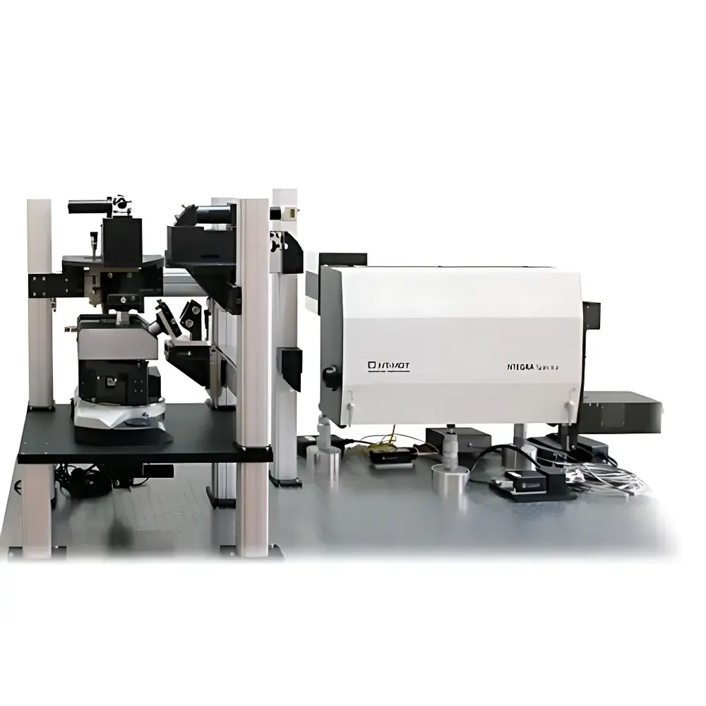
NT-MDT NTEGRA Spectra II Hybrid Atomic Force Microscope with Integrated Confocal Raman and Fluorescence Microscopy
| Brand | NT-MDT |
|---|---|
| Origin | Shanghai, China |
| Manufacturer Type | Authorized Distributor (auniontech) |
| Product Category | Domestic |
| Model | NTEGRA Spectra II |
| Pricing | Upon Request |
Overview
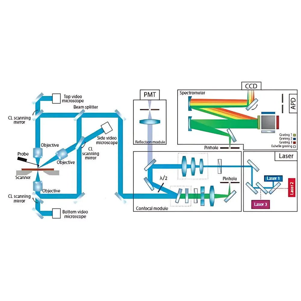
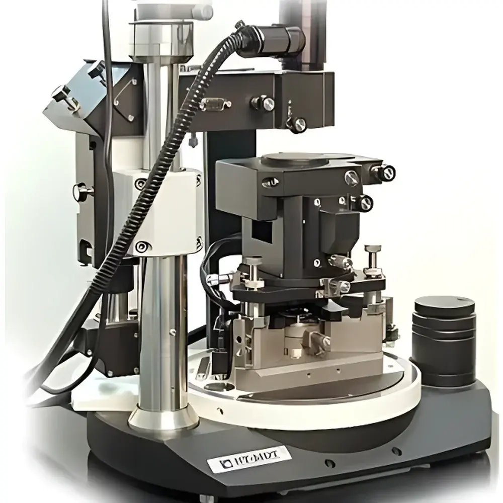
The NT-MDT NTEGRA Spectra II is a high-precision hybrid atomic force microscope engineered for correlative nanoscale characterization. It integrates scanning probe microscopy (SPM) with confocal Raman spectroscopy and fluorescence microscopy in a single, rigid optical-mechanical platform. Based on the principle of dynamic force detection in vacuum or ambient environments—using laser Doppler interferometry for cantilever deflection sensing—the system enables quantitative topographic, mechanical, electrical, and magnetic surface property mapping at sub-nanometer resolution. Its core architecture supports true simultaneous acquisition: AFM topography, phase contrast, and amplitude data are collected in real time while confocal Raman spectra or fluorescence emission maps are acquired from the exact same spatial coordinates. This eliminates registration error and enables unambiguous structure–property–composition correlation—critical for advanced materials research, semiconductor metrology, and life science applications where nanoscale heterogeneity governs functional behavior.
Key Features
- True hybrid multimodal imaging: Co-registered AFM + confocal Raman + fluorescence + SNOM (scanning near-field optical microscopy) in one instrument
- TERS (tip-enhanced Raman spectroscopy) capability with custom-fabricated plasmonic AFM probes acting as nano-antennas for localized field enhancement
- Sub-diffraction optical resolution down to ~10 nm in TERS mode; ~100 nm lateral resolution in SNOM mode
- 30+ operational AFM modes including hybrid Mode™, contact, tapping, phase imaging, force modulation, PFM (piezoresponse), KPFM (Kelvin probe), and conductive AFM
- Integrated motorized XYZ stage with 100 × 100 × 20 µm travel range and closed-loop piezoelectric positioning
- Optical path fully aligned and optimized for excitation/detection at multiple wavelengths (e.g., 532 nm, 633 nm, 785 nm lasers)
- Rigid granite base with active vibration isolation compatibility and acoustic enclosure options
Sample Compatibility & Compliance
The NTEGRA Spectra II accommodates a broad range of solid-state samples—including conductive and insulating thin films, 2D materials (graphene, TMDCs), polymer blends, biological membranes, and semiconductor nanostructures—without requiring conductive coating for most modes. Sample sizes up to 25 mm in diameter and 10 mm in height are supported. The system complies with ISO 25178-601 (areal surface texture parameters) and ASTM E2539 (standard guide for AFM measurements). All software modules support audit trails, electronic signatures, and user-access control per FDA 21 CFR Part 11 requirements when configured in GLP/GMP environments. Instrument calibration protocols follow traceable NIST standards for lateral and vertical scale verification.
Software & Data Management
The Nova software suite provides unified control, real-time visualization, and quantitative analysis across all modalities. It includes dedicated modules for spectral deconvolution (Raman peak fitting), fluorescence lifetime analysis (FLIM), and nanomechanical property extraction (e.g., Young’s modulus mapping via force-distance curve fitting). Data export conforms to HDF5 and TIFF formats with embedded metadata (acquisition parameters, calibration constants, timestamping). Batch processing workflows support automated region-of-interest (ROI) analysis across multi-modal datasets. Raw AFM and spectral files are stored with full provenance, enabling retrospective reprocessing and inter-laboratory reproducibility assessment.
Applications
- Nanoscale chemical mapping of CdS nanowires interfaced with conductive polymers and metal electrodes
- Correlative morphology–crystallinity–strain analysis in perovskite solar cell layers
- Surface potential and charge trapping dynamics in gate dielectrics for FinFET development
- Protein aggregation topology and secondary structure distribution in amyloid fibrils via TERS
- Plasmonic hotspot localization and local dielectric response in metamaterial arrays
- Real-time monitoring of polymer phase separation kinetics under controlled environmental conditions
FAQ
What sample preparation is required for TERS measurements?
Minimal preparation is needed: flat, clean substrates (e.g., Si/SiO₂, ITO, or Au-coated glass) are preferred. No metallization is required for conductive samples; insulators may benefit from ultrathin (<2 nm) Cr or Ti adhesion layers.
Can the system operate in liquid environments?
Yes—fluid cells compatible with electrochemical biasing and temperature control (±0.1°C) are available as optional accessories for in situ AFM-Raman studies.
Is remote operation and data access supported?
The Nova software supports secure client-server architecture over LAN/WAN; role-based web dashboards enable instrument status monitoring and dataset preview without local installation.
How is lateral resolution validated in TERS mode?
Resolution validation follows ISO/IEC 17025-compliant procedures using certified line-width standards (e.g., NIST SRM 2053), with tip radius confirmed by SEM prior to TERS experiments.
Are third-party probes compatible?
While NT-MDT probes are optimized for alignment and plasmonic resonance, standard commercial silicon or silicon nitride probes meeting dimensional tolerances (e.g., ≤10 nm tip radius, ≤2.5 µm cantilever length) can be used in non-TERS AFM modes.


