OSI Optoelectronics J16 Series Ge Infrared Photodetectors
| Brand | OSI Optoelectronics |
|---|---|
| Origin | USA |
| Detector Material | Germanium (Ge) |
| Spectral Range | 800–1800 nm |
| Cooling Options | Uncooled, Thermoelectric (TE), Liquid Nitrogen (LN₂) |
| Active Area Options | 0.25–13 mm² |
| Package Types | TO-8, TO-5, and Custom Mounts |
| Compliance | RoHS-compliant, CE-marked for lab instrumentation use |
| Key Performance Parameters | Shunt Resistance (1–2400 kΩ), Dark Current (0.03–100 µA), NEP (0.02–200 pW/Hz¹ᐟ²), Capacitance (0.03–12 nF), Cutoff Frequency (0.1–400 MHz), Reverse Bias Voltage (up to 400 V) |
Overview
The OSI Optoelectronics J16 Series Germanium (Ge) Infrared Photodetectors are precision-engineered photodiodes optimized for high-sensitivity detection in the near-infrared (NIR) spectral region. Operating across a well-characterized wavelength range of 800–1800 nm, these detectors leverage the intrinsic photoconductive properties of single-crystal germanium to deliver stable responsivity, low temporal noise, and excellent linearity under controlled bias conditions. Unlike silicon-based detectors, Ge exhibits significantly higher quantum efficiency beyond 1000 nm—making it indispensable for applications including Fourier-transform infrared (FTIR) spectroscopy, laser power monitoring at telecom wavelengths (e.g., 1310 nm and 1550 nm), optical coherence tomography (OCT) reference arms, and process analytical technology (PAT) in pharmaceutical and chemical manufacturing. The J16 platform is designed with modular thermal management: uncooled variants provide rapid deployment and low-power operation; thermoelectrically cooled (TEC) configurations reduce dark current by up to two orders of magnitude; and LN₂-cooled versions achieve sub-nanoampere dark current levels required for ultra-low-light spectroscopic measurements.
Key Features
- Three distinct performance families: Low-Capacitance (“HS”), High-Shunt-Resistance (“SC”), and Standard configurations—each engineered for specific signal-to-noise ratio (SNR) and bandwidth trade-offs.
- Seven active area options spanning 0.25 mm² to 13 mm², enabling optimization for either high spatial resolution (small-area) or maximum photon collection (large-area) without compromising electrical interface compatibility.
- Reverse bias voltage support up to 400 V, facilitating improved carrier sweep-out velocity and extended cutoff frequency—critical for time-resolved NIR reflectance and pulsed-laser detection.
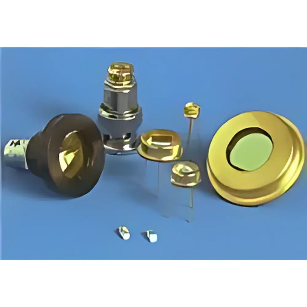
- Hermetically sealed TO-style metal packages (TO-5, TO-8) with AR-coated windows (optional broadband or wavelength-specific coatings) ensure long-term stability and minimal window-induced spectral distortion.
- Comprehensive datasheet documentation includes full DC and AC characterization: shunt resistance (Rsh), dark current (ID), noise-equivalent power (NEP), junction capacitance (Cj), and 3-dB electrical bandwidth—all measured per ANSI Z35.1 and IEC 60747-5-1 standards.
Sample Compatibility & Compliance
J16 Ge detectors integrate seamlessly into OEM spectrometer modules, benchtop FTIR systems, and custom optical setups using standard 50 Ω coaxial or transimpedance amplifier interfaces. Their low thermal mass and compatible mounting footprints allow direct substitution in legacy NIR detector slots. All units comply with RoHS Directive 2011/65/EU and carry CE marking for conformity with the EU Electromagnetic Compatibility (EMC) Directive 2014/30/EU and Low Voltage Directive 2014/35/EU. For regulated environments—including GLP/GMP laboratories and FDA-regulated PAT deployments—the detectors support traceable calibration via NIST-traceable irradiance standards (e.g., NIST SRM 2241), and their stable dark current drift (<0.5% per hour at constant Tc) meets USP requirements for photometric system suitability testing.
Software & Data Management
While the J16 series operates as a passive analog sensor, its electrical output is fully compatible with industry-standard data acquisition platforms—including National Instruments DAQmx, Keysight PathWave, and MATLAB Data Acquisition Toolbox—enabling real-time digitization, spectral averaging, and noise-floor analysis. When integrated with lock-in amplifiers (e.g., Zurich Instruments HF2LI), the detectors support phase-sensitive detection down to sub-pW/√Hz noise floors. All performance parameters are stored in machine-readable format (.csv/.xml) within the manufacturer’s online parametric selector tool, supporting automated BOM generation and SPICE model extraction (via provided .lib files) for circuit-level simulation in Cadence OrCAD or LTspice.
Applications
- FTIR spectrometer detector arrays (single-element scanning or focal-plane array front ends)
- Laser power and energy monitoring in fiber-optic communication test benches (ITU-T G.694.1 compliant)
- NIR process monitoring of polymer melt viscosity, solvent concentration, and API crystallinity in continuous manufacturing lines
- Gas sensing via tunable diode laser absorption spectroscopy (TDLAS) at methane (1650 nm) and CO (1565 nm) absorption lines
- Research-grade optical heterodyne detection in ultrafast spectroscopy and quantum optics experiments
FAQ
What cooling method should I select for my application?
Uncooled detectors suit portable or low-duty-cycle systems where power consumption and form factor are prioritized. TE-cooled variants (−20 °C to −40 °C) are optimal for laboratory FTIR and QC labs requiring stable dark current over multi-hour acquisitions. LN₂-cooled models are reserved for ultra-low-flux applications such as cavity ring-down spectroscopy (CRDS) or single-photon counting in gated detection schemes.
How does active area affect system-level noise performance?
Larger active areas increase photocurrent but also raise junction capacitance and dark current—degrading bandwidth and shot-noise-limited SNR. For high-bandwidth (>10 MHz) or low-light applications, smaller areas (≤1 mm²) combined with high-numerical-aperture focusing optics yield superior NEP and temporal response.
Can I use these detectors with existing transimpedance amplifiers?
Yes—J16 detectors are designed for operation with standard 50 Ω termination or transimpedance gain stages (10⁴–10⁸ V/A). Electrical interface schematics, recommended feedback resistor values, and stability compensation guidelines are provided in Application Note AN-J16-01.
Are calibration certificates available?
Each detector batch undergoes spectral responsivity calibration at three wavelengths (900 nm, 1310 nm, 1550 nm) traceable to NIST. Optional individual unit calibration reports (ISO/IEC 17025 accredited) are available upon request.
Do you offer custom packaging or AR coatings?
Yes—custom window materials (e.g., CaF₂ for extended UV-NIR transmission), anti-reflection coatings (R < 0.5% from 1000–1700 nm), and hermetic ceramic packages with integrated TEC drivers are available under OEM agreements.