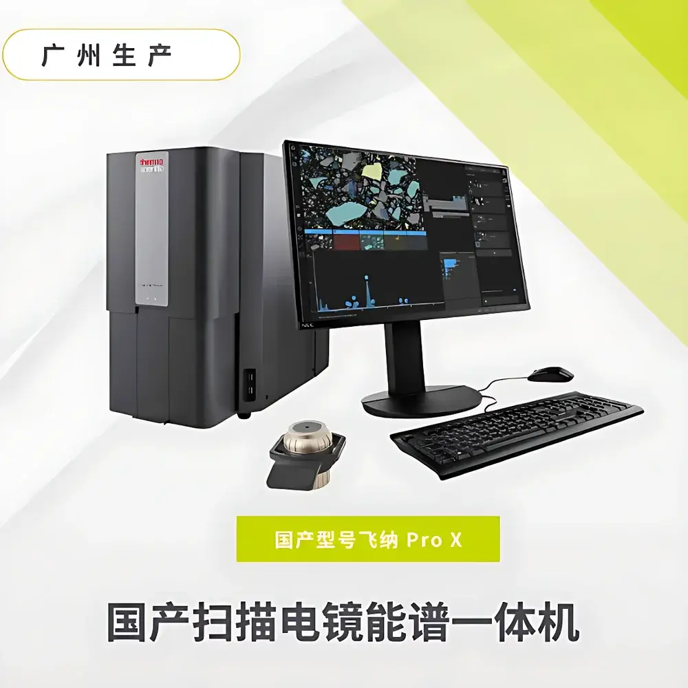
Phenom ProX Desktop Scanning Electron Microscope with Integrated EDS System
| Brand | Phenom |
|---|---|
| Origin | Guangdong, China |
| Manufacturer Type | Authorized Distributor |
| Country of Origin | China |
| Model | Phenom ProX (Domestically Manufactured Variant) |
| Instrument Type | Desktop SEM |
| Electron Source | Cerium Hexaboride (CeB₆) |
| SEM Type | High-Resolution Field-Emission SEM |
| Secondary Electron Resolution | ≤6 nm |
| Maximum Magnification | 350,000× |
| Accelerating Voltage Range | 4.8–20.5 kV |
| Backscattered Electron Resolution | ≤6 nm |
| Sample Stage Capacity | Ø32 mm × H100 mm |
| Vacuum Mode | Standard & Charge Reduction Mode |
| Integrated Detector | Silicon Drift Detector (SDD) EDS |
| Software | Element Identification (EID) with Point, Line, and Area Mapping |
Overview
The Phenom ProX Desktop Scanning Electron Microscope with Integrated EDS System is a fully self-contained, high-performance analytical platform engineered for rapid, high-fidelity surface imaging and quantitative elemental characterization in routine laboratory environments. Unlike conventional floor-standing SEMs requiring dedicated infrastructure, the Phenom ProX employs a compact, vibration-insensitive desktop architecture while maintaining field-emission-level resolution—enabled by its thermally stable cerium hexaboride (CeB₆) electron source and optimized electromagnetic lens system. The instrument operates on the fundamental principles of scanning electron microscopy: a focused electron beam raster-scans the sample surface, generating secondary electrons (SE) for topographic contrast and backscattered electrons (BSE) for atomic number contrast, while simultaneously exciting characteristic X-rays used for energy-dispersive spectroscopy (EDS). This dual-modality design allows concurrent acquisition of morphological and compositional data without sample relocation or vacuum break—critical for time-sensitive QC workflows, materials forensics, and academic research where spatial correlation between structure and chemistry is essential.
Key Features
- Sub-6 nm secondary electron and backscattered electron resolution at optimal accelerating voltages, enabling visualization of nanoscale features including grain boundaries, nanoparticle dispersion, and coating uniformity.
- CeB₆ electron source delivering high brightness and exceptional beam stability over extended acquisition periods—reducing drift-related artifacts during mapping or time-lapse analysis.
- Integrated silicon drift detector (SDD) EDS system with real-time spectral processing, optimized for light-element detection (B to U) and quantitative ZAF correction algorithms compliant with ISO 14782 and ASTM E1508 standards.
- Intuitive, wizard-driven Element Identification (EID) software supporting point analysis, line scans, and high-resolution elemental mapping (up to 1024 × 1024 pixels) with automatic peak deconvolution and matrix effect compensation.
- Dual-vacuum operation modes: standard high-vacuum mode for conductive samples and charge-reduction mode for insulating or beam-sensitive specimens—eliminating the need for metal sputter coating in many applications.
- Onboard color optical navigation camera for fast, low-magnification sample positioning and region-of-interest selection—reducing setup time by >50% compared to traditional SEM workflows.
Sample Compatibility & Compliance
The Phenom ProX accommodates specimens up to 32 mm in diameter and 100 mm in height, supporting bulk solids, polished cross-sections, powders, biological tissues (with appropriate preparation), and coated substrates. Its modular chamber design permits rapid sample exchange under partial vacuum, minimizing downtime between analyses. All hardware and firmware comply with IEC 61000-6-3 (EMC emissions) and IEC 61000-6-2 (immunity) standards. The EDS software implements audit-trail functionality aligned with GLP and GMP requirements, including user authentication, timestamped session logs, and immutable data export (CSV, TIFF, SPC, and EDAX-compatible .eds formats). Full traceability meets FDA 21 CFR Part 11 criteria when deployed with validated network configurations and electronic signature protocols.
Software & Data Management
Element Identification (EID) software provides a unified interface for both imaging and microanalysis—no external modules or license dongles required. Acquired spectra are processed using a proprietary noise-filtering algorithm that enhances signal-to-background ratio without compromising peak fidelity. Quantitative analysis supports standardless and standards-based calibration workflows, with optional integration into LIMS via ODBC-compliant database connectors. All raw images, spectra, and maps are stored in vendor-neutral formats with embedded metadata (accelerating voltage, working distance, dwell time, detector geometry), ensuring long-term reproducibility and third-party compatibility. Batch export functions support automated report generation—including annotated PDFs with overlayed elemental maps and statistical summaries per ROI.
Applications
- Materials Science: Phase identification in alloys, inclusion analysis in steels, porosity quantification in additive-manufactured parts, and interfacial characterization in multilayer thin films.
- Geology & Mining: Mineral phase discrimination, grain size distribution analysis, and geochemical mapping of ore samples without carbon coating.
- Electronics: Failure analysis of solder joints, contamination identification on PCBs, and cross-sectional inspection of dielectric layers.
- Life Sciences: Morphometric analysis of freeze-dried cells, vascular network reconstruction in tissue scaffolds, and elemental co-localization in calcified biominerals.
- Quality Control: Incoming raw material verification, coating thickness validation, and defect root-cause analysis across automotive, aerospace, and medical device manufacturing lines.
FAQ
Is the domestically manufactured Phenom ProX equivalent in performance to the Netherlands-assembled unit?
Yes. Units produced at the Guangzhou facility undergo identical factory calibration, optical alignment, and resolution verification per Phenom’s global quality protocol (ISO 9001:2015 certified production line). All specifications—including 6 nm SE resolution and CeB₆ source lifetime—are maintained without compromise.
Does the integrated EDS system require liquid nitrogen cooling?
No. The SDD detector uses Peltier-based thermoelectric cooling, eliminating cryogen handling and enabling continuous operation in standard laboratory environments.
Can the system analyze non-conductive samples without sputter coating?
Yes. The charge-reduction vacuum mode, combined with low-kV imaging (down to 4.8 kV) and beam deceleration technology, enables direct imaging and EDS acquisition on polymers, ceramics, and biological specimens.
What level of training and technical support is provided?
Phenom offers on-site installation qualification (IQ), operator certification workshops, and remote troubleshooting via secure screen-sharing. All software updates and firmware patches are delivered automatically through the Phenom Connect portal.
Is data export compliant with regulatory submission requirements?
Yes. Raw data files include full acquisition metadata, and the EID software supports 21 CFR Part 11–compliant electronic signatures, audit trails, and role-based access control when configured on a domain-authenticated Windows environment.


