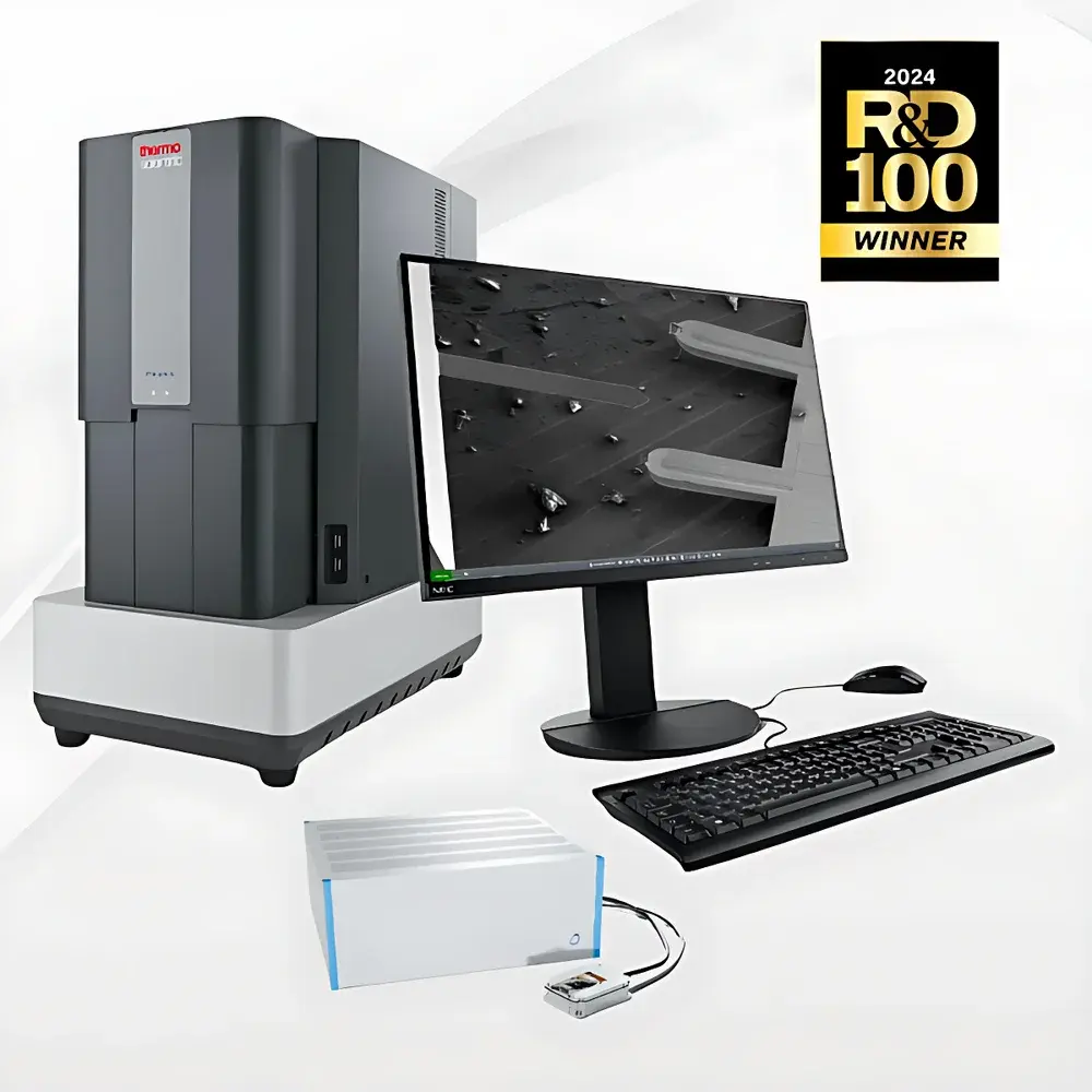
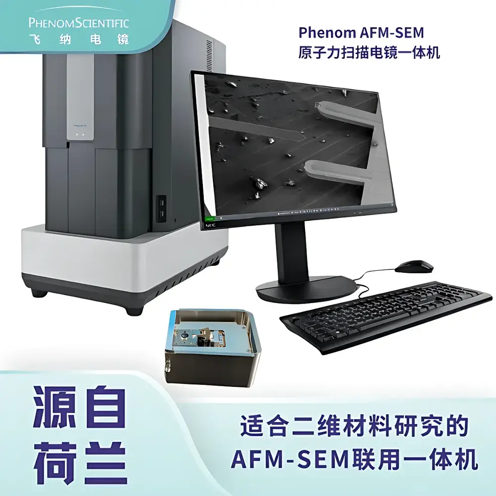
Phenom SEM-AFM Hybrid Atomic Force and Scanning Electron Microscope for 2D Materials Research
| Brand | Phenom |
|---|---|
| Origin | Netherlands |
| Model | SEM-AFM |
| Instrument Type | Benchtop SEM-AFM Integrated System |
| Electron Source | Cerium Hexaboride (CeB₆) |
| Maximum Sample Dimensions | 21 mm × 11 mm × 8 mm |
| Sample Weight Limit | 100 g |
| Open-Loop Scan Range | 100 µm × 100 µm × 20 µm |
| Closed-Loop Scan Range | 80 µm × 80 µm × 16 µm |
| Spatial Resolution (XY/Z) | 0.2 nm × 0.2 nm / 0.04 nm |
| Compatible Modes | Topography, Roughness, CAFM, KPFM, FMM, PFM, EFM, Force–Distance (F–z), Current–Voltage (I–V) |
Overview
The Phenom SEM-AFM Hybrid Atomic Force and Scanning Electron Microscope is an engineered benchtop platform that co-localizes high-resolution scanning electron microscopy (SEM) and atomic force microscopy (AFM) within a single vacuum-compatible chamber. Unlike conventional correlative workflows requiring sample transfer between separate instruments—introducing positional uncertainty, contamination risk, and time delay—this integrated system enables true spatially registered multimodal characterization of 2D materials at nanoscale precision. The instrument leverages a thermionic CeB₆ electron source to deliver stable, high-brightness imaging up to 5 kV accelerating voltage, while the AFM module operates in ultra-high vacuum or low-vacuum conditions compatible with SEM operation. Measurement principles include secondary electron detection (SEM), tunneling current and electrostatic force sensing (CAFM/KPFM/EFM), piezoelectric response mapping (PFM), and mechanical deflection-based topographic reconstruction (contact/tapping mode). Designed specifically for layered van der Waals materials—including transition metal dichalcogenides (TMDCs), graphene derivatives, hexagonal boron nitride (h-BN), and MXenes—the system supports quantitative structure–property correlation across morphological, electrical, electrostatic, ferroelectric, and nanomechanical domains.
Key Features
- Benchtop integration of SEM and AFM in a shared sample chamber, eliminating stage repositioning errors and enabling sub-100 nm registration accuracy between modalities
- CeB₆ electron gun offering superior brightness and lifetime over tungsten filaments, optimized for low-kV imaging of beam-sensitive 2D crystals
- Simultaneous acquisition of SEM secondary electron images and AFM topography, phase, amplitude, and force–distance data under identical environmental conditions
- Closed-loop piezoelectric scanner with 80 µm × 80 µm × 16 µm range and <0.04 nm Z-resolution, calibrated via on-chip interferometric feedback
- Multi-functional probe compatibility: conductive diamond, Pt/Ir-coated, and Ti/Ir-coated cantilevers for CAFM, KPFM, EFM, and PFM
- Integrated vacuum interlock and pressure monitoring to maintain ≤10⁻³ mbar during combined operation, minimizing surface adsorption and drift
Sample Compatibility & Compliance
The system accommodates standard 2D material substrates including Si/SiO₂ wafers, TEM grids, mica flakes, and polymer-supported transfers, with maximum dimensions of 21 mm × 11 mm × 8 mm and mass limit of 100 g. All stages are motorized and software-synchronized to ensure repeatable positioning across sessions. The instrument complies with IEC 61000-6-3 (EMC emission standards) and IEC 61010-1 (safety requirements for laboratory equipment). Data acquisition protocols support GLP-compliant metadata tagging, including timestamp, operator ID, vacuum status, detector gain, and scan parameters—enabling traceability in regulated R&D environments. While not certified for FDA 21 CFR Part 11 out-of-the-box, audit trails and user-access controls can be configured per institutional IT policies.
Software & Data Management
Control and analysis are performed via Phenom’s proprietary SEM-AFM Suite v4.x, a Windows-based application supporting synchronized acquisition, real-time overlay rendering, and cross-modal pixel-matched data export (TIFF, HDF5, Gwyddion-compatible formats). The software implements automated tip approach routines, thermal drift compensation algorithms, and batch processing for multi-region AFM-SEM correlation. Raw datasets retain full metadata headers compliant with FAIR (Findable, Accessible, Interoperable, Reusable) principles. Exported maps support third-party quantification in MATLAB, Python (via PySPM), or commercial packages such as Gwyddion and SPIP. All measurement logs are archived with SHA-256 checksums and configurable retention periods.
Applications
This hybrid platform is routinely deployed in academic and industrial labs investigating structure–function relationships in 2D heterostructures. Typical use cases include: correlating MoS₂ grain boundary location (SEM) with local work function variation (KPFM) and nanoscale conductivity (CAFM); mapping ferroelectric domain switching in α-In₂Se₃ under bias (PFM + SEM); quantifying strain-induced bandgap shifts via simultaneous topography (AFM) and cathodoluminescence (if equipped with optional CL add-on); and evaluating layer stacking order in twisted bilayer graphene using phase contrast (AFM) and edge contrast (SEM). It further supports failure analysis of 2D-integrated transistors, interface trap density estimation at dielectric/2D semiconductor junctions, and in situ thermal/electrical stimulation experiments.
FAQ
Can the system operate both SEM and AFM simultaneously without signal interference?
Yes—the SEM column and AFM head are electromagnetically shielded and acoustically isolated; real-time dual-mode acquisition has been validated for continuous 30-minute sessions with <2% SNR degradation.
Is cryogenic or heating stage integration supported?
The chamber features two standardized feedthrough ports (electrical + thermal) compatible with commercially available cryo- or heating stages (e.g., Linkam LTS420), though vacuum compatibility must be verified per vendor specifications.
What level of training is required to achieve reliable multimodal correlation?
Operators with foundational SEM or AFM experience typically complete competency certification within three supervised sessions; full workflow autonomy—including tip calibration, drift correction, and overlay registration—is achievable within one week.
Are probe exchange and alignment procedures automated?
Probe loading is manual but guided by on-screen visual alignment aids; laser alignment is semi-automated via iterative reflection optimization, reducing setup time to under 8 minutes per cantilever type.
Does the system support automated region-of-interest (ROI) navigation across large-area samples?
Yes—low-magnification SEM survey imaging (up to 1 mm field of view) enables coordinate-based ROI targeting for subsequent high-res AFM/SEM scans, with positional repeatability better than ±200 nm.


