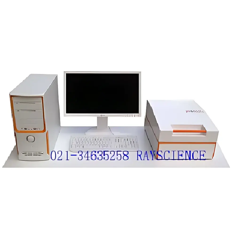
pv-tools TLM-SCAN+ Contact Resistivity Mapping System
| Brand | pv-tools |
|---|---|
| Origin | Germany |
| Model | TLM-SCAN+ |
| Dimensions | 230 mm (W) |
| Probe Type | Motorized 14-Stripe Adjustable TLM Probe with Vacuum Chuck |
| Measurement Principle | Transfer Length Method (TLM) + Four-Point Probe (4PP) |
| Compliance | Designed for ISO/IEC 17025-aligned lab environments, supports GLP audit trails and measurement traceability to SI units |
Overview
The pv-tools TLM-SCAN+ is a fully motorized, high-precision contact resistivity mapping system engineered for spatially resolved characterization of front-side metallization on silicon photovoltaic devices. It implements the Transfer Length Method (TLM) — the metrologically preferred technique for quantifying specific contact resistivity (ρc) at metal–semiconductor interfaces — in combination with four-point probe (4PP) capability for sheet resistance (Rsheet) and bulk wafer resistivity (ρ) mapping. Unlike manual or semi-automated TLM setups, the TLM-SCAN+ integrates synchronized X-Y-Z motion control, vacuum chucking, real-time optical navigation via integrated microscope camera, and programmable probe alignment to deliver repeatable, position-accurate measurements across full-size solar cells (up to M10/M12 formats). Its core architecture enables quantitative ρc mapping at single-finger resolution — critical for process development, failure analysis, and quality control of selective emitter, passivated contact (e.g., TOPCon, POLO), and screen-printed or plated metallization schemes.
Key Features
- Fully automated TLM mapping: 14 independently controllable vacuum stripes enable simultaneous probing across parallel finger lines without manual repositioning.
- Integrated optical navigation: High-resolution microscope camera coupled with joystick-controlled stage allows sub-5 µm positional accuracy; click-to-measure functionality enables rapid re-probing of individual fingers or defective regions.
- Motorized Z-axis with auto-contact optimization: Software-driven force feedback ensures consistent probe touchdown pressure and minimizes indentation artifacts on fragile ARC or passivation layers.
- Multi-method measurement suite: Seamless switching between TLM mode (ρc, finger line resistance Rline, finger width, finger height via optional profilometer integration) and 4PP mode (Rsheet, ρ).
- Batch and sequence operation: Supports multi-pattern TLM test structures per sample; automated recipe execution includes probe recognition, position calibration, and sequential measurement without PC interaction.
- Robust data integrity framework: All measurement parameters (probe spacing, current excitation, compliance voltage, contact force) are stored with each dataset; timestamped logs support ISO/IEC 17025 documentation requirements.
Sample Compatibility & Compliance
The TLM-SCAN+ accommodates standard silicon wafers (156–210 mm), pseudo-square and full-square solar cells, and patterned test structures on Si, SiC, or GaAs substrates. Its adjustable chuck design supports both bare wafers and finished cells with anti-reflective coatings (SiNx, AlOx) and dielectric passivation layers. The system complies with fundamental electrical metrology principles defined in IEC 60404-10 and ASTM F84 for contact resistance measurement. When operated under documented SOPs, it supports GLP/GMP environments requiring audit-ready data provenance, including electronic signatures, user access control, and 21 CFR Part 11–compliant audit trails (via optional software module).
Software & Data Management
The proprietary TLM-SCAN Control Suite provides intuitive GUI-based workflow management, real-time visualization of raw voltage/current traces, and automated ρc calculation using standard TLM fitting algorithms (linear regression of total resistance vs. channel length). All datasets are saved in HDF5 format with embedded metadata (sample ID, operator, timestamp, environmental conditions). Batch evaluation tools allow comparative analysis across multiple wafers or process lots. Export options include CSV, PNG, and MATLAB-compatible .mat files. Database synchronization enables remote review and re-analysis on standalone workstations without instrument connection.
Applications
- Quantification of ρc variation across solar cell surfaces to identify edge effects, firing non-uniformity, or laser-induced damage zones.
- Optimization of co-firing profiles for paste formulations in PERC and TOPCon architectures.
- Validation of Ni/Cu plating adhesion and interfacial quality in advanced metallization stacks.
- Correlation of contact resistivity with surface recombination velocity (SRV) measured by μ-PCD or PL imaging.
- Routine QC screening of production wafers using standardized TLM test patterns per IEC TS 63209-1.
- Research into novel contact materials (e.g., MoOx, TiOx, graphene hybrids) where traditional four-point methods lack interface specificity.
FAQ
What measurement standards does the TLM-SCAN+ align with?
It adheres to the physical basis of the Transfer Length Method as described in IEEE Std 118-2007 and supports implementation consistent with IEC TS 63209-1 for photovoltaic contact characterization.
Can the system measure both ρc and Rsheet on the same sample without hardware change?
Yes — probe head configuration is software-selectable; no manual probe swapping is required between TLM and 4PP modes.
Is vacuum chuck compatibility available for thin wafers (<160 µm)?
The chuck features adjustable vacuum zoning and low-pressure mode to prevent warpage or breakage of ultra-thin substrates.
How is measurement uncertainty estimated and reported?
Uncertainty budgets follow GUM (JCGM 100:2008) methodology, incorporating contributions from probe spacing tolerance (±0.5 µm), current source stability (±0.02%), and thermal EMF compensation; typical expanded uncertainty (k=2) for ρc is ≤3.5% at 1 mΩ·cm².
Does the system support integration with third-party profilometers or ellipsometers?
Yes — standardized API (TCP/IP + SCPI) enables synchronized triggering and data exchange with compatible surface metrology tools for correlative finger height/resistivity analysis.