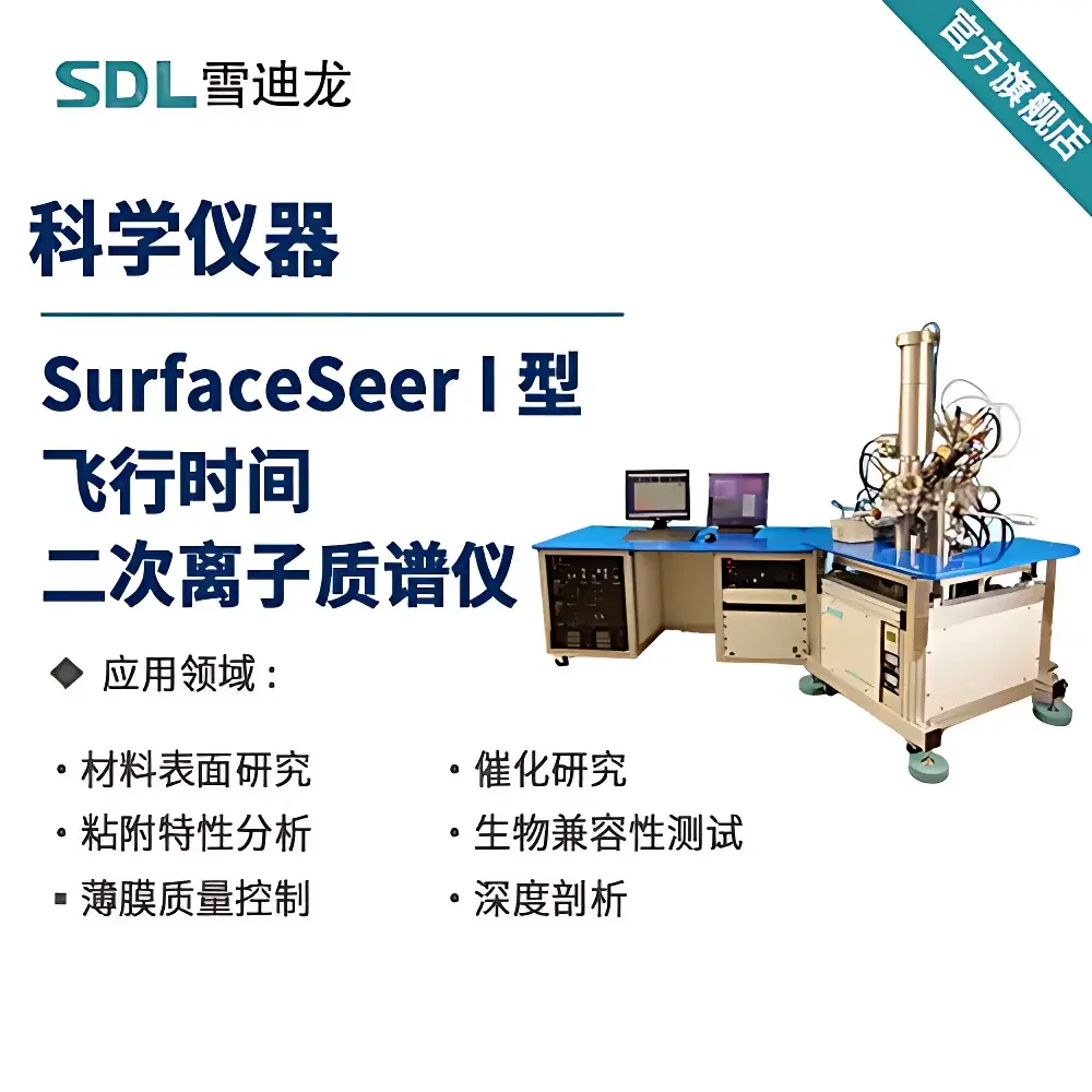
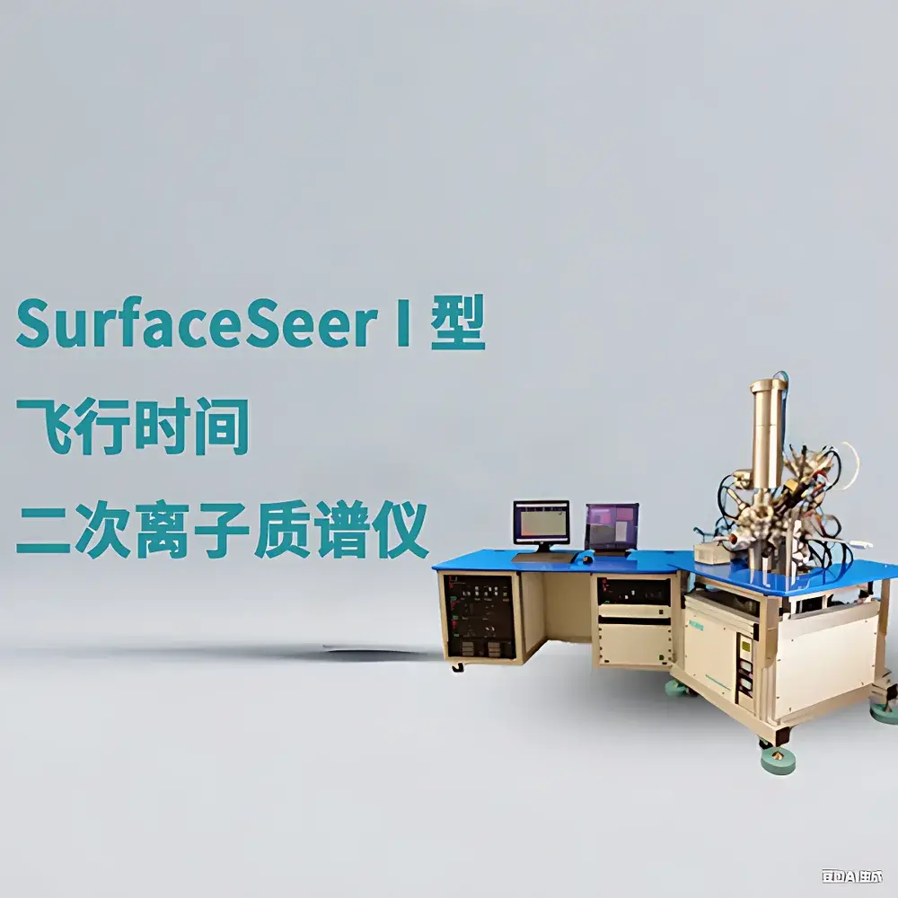
SDL SurfaceSeer I Time-of-Flight Secondary Ion Mass Spectrometer
| Brand | SDL |
|---|---|
| Origin | United Kingdom |
| Manufacturer Type | Original Equipment Manufacturer (OEM) |
| Product Category | Imported Instrument |
| Model | SurfaceSeer I |
| Mass Analysis Range | 1000–10000 amu |
| Mass Resolution | >3,000 m/δm (FWHM) |
| Analyzer Type | Time-of-Flight (TOF) |
Overview
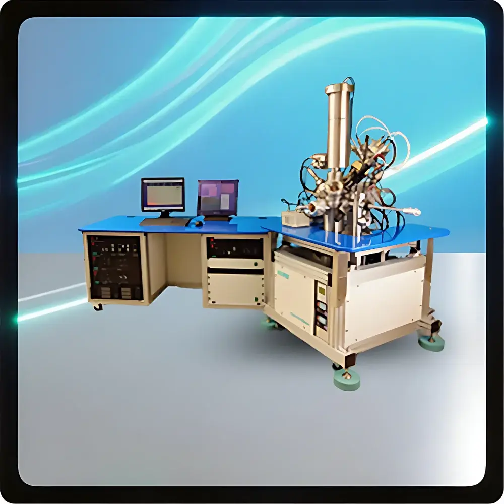
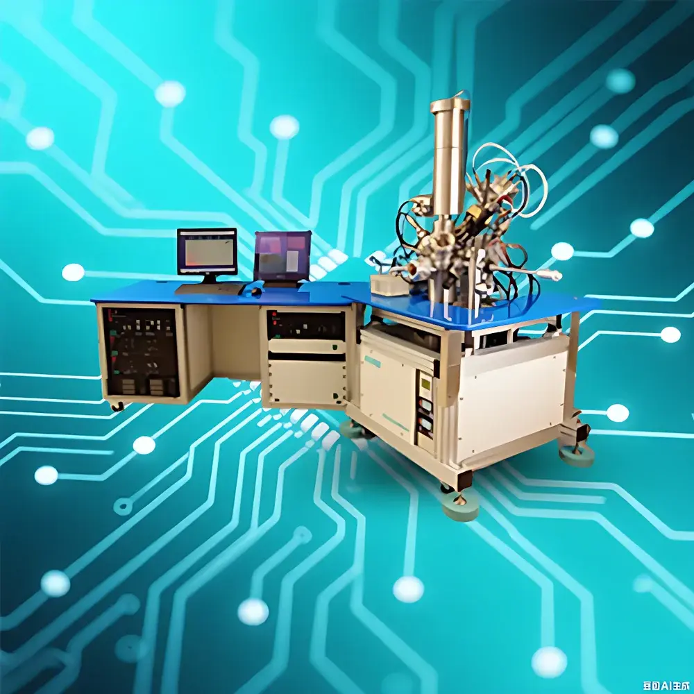
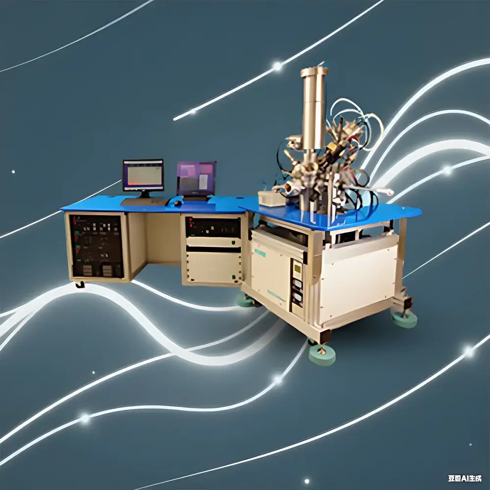
The SDL SurfaceSeer I is a high-performance time-of-flight secondary ion mass spectrometer (TOF-SIMS) engineered for surface-sensitive elemental and molecular characterization of solid materials at sub-monolayer sensitivity. Based on the fundamental principle of sputter-induced secondary ion emission followed by orthogonal acceleration and time-resolved mass separation, the SurfaceSeer I delivers high mass resolution, excellent mass accuracy, and spatially resolved chemical imaging capabilities. Designed for research laboratories and industrial R&D centers requiring trace-level surface contamination analysis, thin-film composition mapping, organic/inorganic interface characterization, and depth profiling of functional coatings, the instrument integrates a pulsed primary ion source with a reflectron-enhanced TOF mass analyzer to achieve robust signal reproducibility and low detection limits across the full mass range (1000–10000 amu). Its architecture supports ultra-high vacuum (UHV) operation (<1×10⁻⁹ mbar), ensuring minimal background interference and long-term stability during extended acquisition sequences.
Key Features
- Time-of-flight mass analyzer with reflectron correction, enabling >3,000 m/δm resolution (FWHM) at mid-mass range and linear dynamic response over five orders of magnitude
- Dual-mode operation: static SIMS for molecular surface mapping and dynamic SIMS for controlled depth profiling with nanoscale depth resolution
- Ultra-high vacuum sample chamber (<1×10⁻⁹ mbar base pressure) with integrated cryo-shielding and in-situ sample cleaning capability
- Automated sample stage with XYZ precision motion control (±0.1 µm repeatability) and tilt/rotation for angular-resolved analysis
- Integrated electron flood gun for charge compensation on insulating samples, ensuring stable spectral acquisition without surface charging artifacts
- Modular ion source design supporting Bi+, C60+, and Ar-GCIB (gas cluster ion beam) options for optimized sputter yield and molecular fragmentation control
Sample Compatibility & Compliance
The SurfaceSeer I accommodates conductive, semiconductive, and insulating solid samples—including metals, oxides, polymers, biological tissues, and multilayer semiconductor wafers—up to 25 mm in diameter and 10 mm in thickness. Sample introduction is performed via load-lock system to maintain UHV integrity. The instrument complies with ISO/IEC 17025:2017 requirements for analytical laboratory competence and supports audit-ready data acquisition workflows aligned with GLP and GMP principles. All spectral data files are timestamped, digitally signed, and structured according to ASTM E1819–22 standards for SIMS data reporting. Instrument calibration protocols follow NIST-traceable reference materials (e.g., Si wafer with implanted As, Au standard films), and routine performance verification adheres to IEC 61000-4-3 for electromagnetic compatibility.
Software & Data Management
Controlled via SDL’s proprietary SurfaceSuite™ software suite, the SurfaceSeer I provides an intuitive, role-based interface for method development, real-time spectral monitoring, and multidimensional data reconstruction. The software supports automated batch processing of large-area imaging datasets (up to 1024 × 1024 pixel maps), PCA-based spectral clustering, and overlay correlation with complementary techniques (e.g., XPS, AFM). All raw and processed data are stored in vendor-neutral HDF5 format, ensuring long-term archival integrity and third-party interoperability. Audit trail functionality records user actions, parameter changes, and calibration events in accordance with FDA 21 CFR Part 11 requirements. Optional integration with LIMS platforms is supported via RESTful API and OPC UA protocols.
Applications
- Surface chemistry analysis of catalysts, battery electrode interfaces, and corrosion layers
- Molecular mapping of pharmaceutical tablet coatings and polymer blend phase separation
- Depth profiling of high-k dielectrics, gate stacks, and 3D NAND memory structures
- Contamination identification in semiconductor fab environments (e.g., metal residues, organic residues)
- Chemical imaging of biomaterial surfaces, including protein adsorption patterns and lipid domain distribution
- Forensic analysis of trace evidence (paint chips, gunshot residue, microplastics)
FAQ
What is the typical mass calibration stability over a 24-hour acquisition?
Calibration drift remains within ±0.05 amu when using internal lock-mass referencing and ambient temperature stabilization (±0.5 °C).
Does the SurfaceSeer I support quantitative analysis?
Yes—relative quantification is achievable using matrix-matched standards; absolute quantification requires certified reference materials and ion yield correction models validated per ISO 18115-2.
Can the system be upgraded to include gas cluster ion beam (GCIB) sputtering?
Yes—the platform features a field-upgradable GCIB module compatible with Arn+ (n = 500–5000) and CO2n+ clusters for damage-free organic depth profiling.
Is remote operation supported for multi-user lab environments?
Remote monitoring and method queuing are enabled via TLS-secured web interface; full remote control requires on-premise VPN configuration and administrator privileges.
What maintenance intervals are recommended for optimal TOF performance?
Vacuum system inspection every 6 months; detector gain recalibration every 12 months; primary ion source replacement every 18–24 months under standard usage (≤8 h/day).