A-Z Series Polycrystalline Metal Substrates (Hefei Kejing Brand)
| Brand | Hefei Kejing |
|---|---|
| Origin | Anhui, China |
| Manufacturer Type | Authorized Distributor |
| Product Origin | Domestic (China) |
| Model | A-Z Polycrystalline Metal Substrates |
| Pricing | Available Upon Request |
Overview
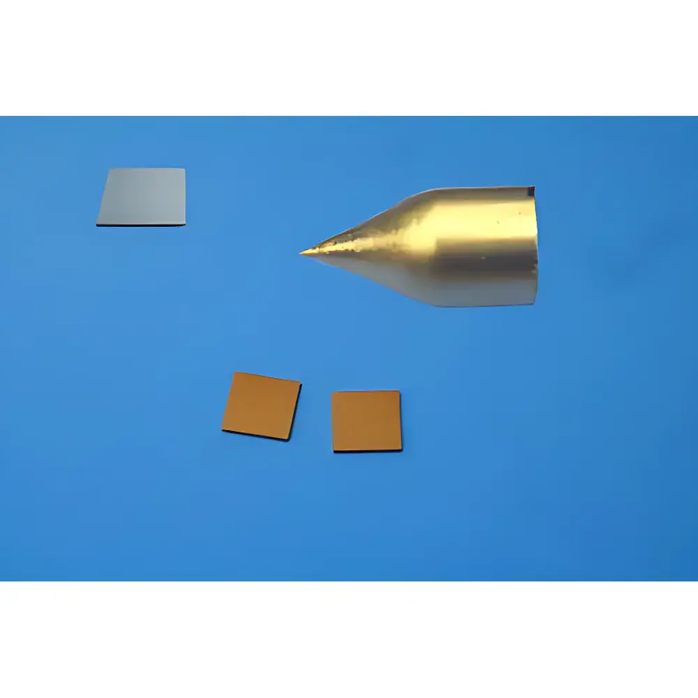
The A-Z Series Polycrystalline Metal Substrates are high-purity, vacuum-packaged metallic base materials engineered for use in thin-film deposition, physical vapor deposition (PVD), sputtering target preparation, surface science studies, and calibration reference applications. Each substrate is fabricated from polycrystalline bulk metal—exhibiting isotropic mechanical and thermal properties—and is not single-crystal; thus, they provide cost-effective, reproducible platforms where crystallographic orientation is non-critical. Manufactured under controlled cleanroom conditions (Class 1000 fabrication environment, Class 100 clean bag packaging), these substrates minimize particulate contamination and native oxide formation prior to use. Their polycrystalline microstructure ensures uniform sputter yield and consistent etch behavior across multiple process cycles—key requirements in R&D laboratories and pilot-scale coating facilities.
Key Features
- Comprehensive elemental coverage: Includes Al, Au, Cu, Cr, Co, Er, Fe, Mo, Hf, Ni, Nb, Ti, Ta, W, Y, Zr, plus ultra-high-purity variants of Be (3N5–5N), Ca (3N5–5N), and Mg (3N5–5N)
- Controlled purity grades: Standard offerings range from 99.95% (3N5) to 99.999% (5N); certified assay reports available upon request
- Surface finish options: As-rolled, electropolished, or double-side lapped finishes—each with documented Ra values and flatness tolerances
- Dimensional flexibility: Available in diameters from 10 mm to 100 mm and thicknesses from 0.25 mm to 5.0 mm; custom geometries (e.g., rectangles, annuli) supported
- Traceable packaging: Vacuum-sealed in Class 100 polyethylene clean bags inside stainless steel vacuum storage boxes with desiccant and O₂ indicator
- Oxidation mitigation protocol: All substrates shipped with inert gas backfill (Ar or N₂) and include handling guidelines compliant with ASTM F1470-22 for metallic substrate storage
Sample Compatibility & Compliance
These substrates are compatible with electron-beam evaporation, DC/RF magnetron sputtering, thermal evaporation, and pulsed laser deposition (PLD) systems. Surface oxide content is minimized through post-annealing in ultra-high vacuum (<1×10⁻⁷ Torr) prior to packaging—verified via XPS depth profiling on representative lots. Material certifications conform to ISO 9001:2015 manufacturing protocols. For regulated environments, documentation packages support GLP and GMP workflows, including lot-specific CoA (Certificate of Analysis), traceable metallurgical mill test reports, and residual gas analysis (RGA) data. While not intended for direct FDA-regulated device manufacturing, substrates meet raw material specifications referenced in USP particulate matter testing and ASTM E2651-21 for metallic reference standards.
Software & Data Management
No embedded firmware or proprietary software is associated with these passive substrates. However, full digital traceability is provided: each lot includes a QR-coded label linking to an online portal containing downloadable PDFs of CoA, dimensional inspection reports, surface roughness maps (profilometry), and oxidation state verification (XPS survey scans). Audit trails comply with 21 CFR Part 11 requirements for electronic records when accessed via institutional SSO-authenticated accounts. Raw metrology datasets (e.g., AFM topography, EDS elemental maps) are available upon formal data request under NDA.
Applications
- Calibration references for X-ray fluorescence (XRF) and energy-dispersive X-ray spectroscopy (EDS)
- Baseline substrates for adhesion testing (ASTM D3359, ISO 2409) of metallic coatings
- Thermal conductivity benchmarking in transient plane source (TPS) measurements
- Reference electrodes in electrochemical impedance spectroscopy (EIS) cell development
- Mask alignment targets in photolithography process qualification
- Substrates for resistivity mapping (four-point probe per ASTM F84-22) and Hall effect characterization
- Model systems in corrosion science studies (e.g., galvanic coupling arrays per ASTM G71)
FAQ
Are these substrates suitable for UHV (ultra-high vacuum) chamber loading without pre-baking?
Yes—substrates are packaged under ≤1×10⁻³ Torr and undergo final outgassing stabilization at 150°C for 4 hours prior to sealing. Residual gas analysis confirms total pressure rise <5×10⁻⁹ Torr·L/s after 24-hr bakeout at 200°C.
Can I obtain substrates with pre-deposited seed layers (e.g., TiW adhesion layers)?
Custom metallization—including bilayer or trilayer stacks—is available under NRE agreement; lead time extends by 3–4 weeks.
Do you supply substrates with certified surface roughness (Ra) and flatness (PV) values?
Yes—standard electropolished substrates include CMM-measured flatness (≤10 µm PV over 50 mm) and profilometer-verified Ra (≤0.02 µm); metrology reports are lot-specific.
What is the recommended storage lifetime before degradation occurs?
When maintained in original vacuum packaging at ≤25°C and <30% RH, shelf life is ≥24 months; opened substrates must be transferred to active vacuum storage within 2 hours.
Is material traceability extended to melt origin and rolling history?
Yes—full upstream traceability (ingot heat number, hot/cold rolling pass logs, annealing atmosphere composition) is included in extended CoA packages for qualified purchasers.


