Sigray APEX XCT-150 Industrial Micro-CT System
| Brand | Sigray |
|---|---|
| Origin | Shanghai, China |
| Model | APEX XCT-150 |
| X-ray Source | Sealed-tube nanofocus transmission source (30–160 kVp, 25 W, tungsten target) |
| Spatial Resolution | 0.5 µm (uncompromised across full 300 mm diameter field of view) |
| Minimum Voxel Size | 70 nm |
| Detector | 6.7 MP, 50 µm pixel pitch, 9 FPS, 14 × 11 cm active area |
| Optical Alignment Camera | 16 MP visible-light camera |
| Software Suite | Sigray3D acquisition platform + GigaRecon iterative reconstruction engine |
| Reconstruct Speed | <45 s for 2048 × 2048 × 2200 dataset |
| Sample Handling | Automated Sample Handling Robot (SHR), supports up to 20 samples per batch |
| Motion Stage | XYZ travel 100 × 100 × 20 mm (customizable extension available) |
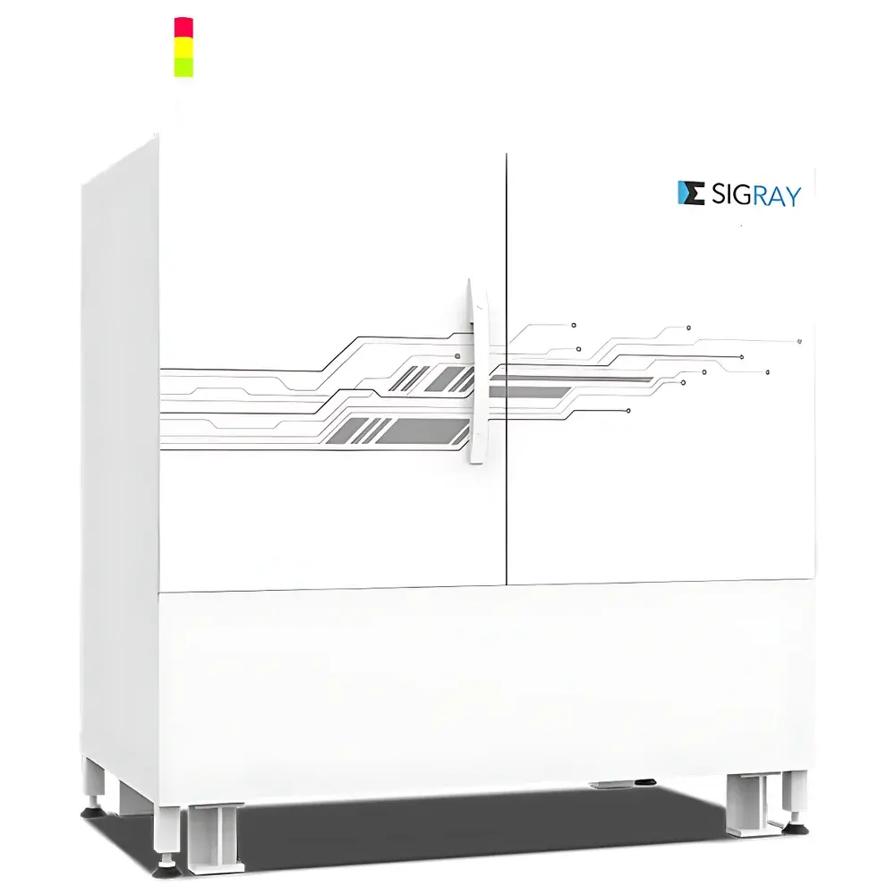
| System Dimensions | 2.24 m (L) × 1.24 m (W) × 2.34 m (H) |
| Operating Systems | Dual-station architecture — Windows-based GUI workstation + Linux-based real-time control workstation (EPICS-compatible) |
| Compliance | Designed for GLP/GMP-aligned lab environments |
Overview
The Sigray APEX XCT-150 is an industrial-grade micro-computed tomography (micro-CT) system engineered for high-fidelity, non-destructive 3D imaging of semiconductor packages, printed circuit boards (PCBs), wafers, and advanced heterogeneous integrated devices. Unlike conventional cone-beam CT systems constrained by geometric magnification limits and beam-hardening artifacts, the APEX XCT-150 employs a proprietary parallel-beam nanofocus transmission architecture with fixed-source–detector geometry. This design decouples spatial resolution from sample size—enabling consistent 0.5 µm isotropic resolution across the entire 300 mm diameter field of view without trade-offs in signal-to-noise ratio or acquisition time. The system integrates a sealed-tube tungsten-target X-ray source (30–160 kVp, 25 W), optimized for stable, maintenance-free operation at high photon flux, and a large-area, high-quantum-efficiency detector capable of sustained performance at energies up to 160 kV. Its physical architecture eliminates common CT artifacts—including beam hardening, photon starvation, metal-induced streaking, and edge-shading—making it uniquely suited for metrology-critical applications in failure analysis (FA), process development, and inline quality assurance.
Key Features
- Nanofocus Transmission Geometry: Fixed-source–detector alignment ensures constant magnification and resolution independence from sample dimensions—critical for full-package FA and wafer-level inspection.
- 0.5 µm Resolution Across Full FOV: Achieved without binning or interpolation; validated via NIST-traceable line-pair phantoms and verified on sub-5 µm TSVs and RDL features.
- Time-Invariant Acquisition: Scan duration remains constant regardless of sample size—e.g., 27 minutes for full SSD imaging, 34 minutes for GPU+PCB at 1.0 µm voxel, 6 minutes for 300 mm wafer defect screening.
- Artifact-Free Imaging Engine: Eliminates beam-hardening-induced cupping, metal streaking, and partial-volume blurring through monochromatic-like spectral response and optimized detector quantum efficiency.
- Dual-OS Control Architecture: Windows-based Sigray3D GUI for intuitive alignment and acquisition planning; Linux-based real-time control node (EPICS-integrated) for deterministic, 24/7 unattended operation.
- Automated Sample Handling: Integrated Sample Handling Robot (SHR) enables fully autonomous multi-sample workflows—including overnight runs and weekend scheduling—with full audit-trail logging.
Sample Compatibility & Compliance
The APEX XCT-150 accommodates samples up to 300 mm in diameter and 20 mm in height—covering full 300 mm wafers, stacked-die packages, server-grade PCBs, and complete consumer electronics assemblies (e.g., iPhone 14 Pro logic modules). Its mechanical stage provides 100 mm × 100 mm × 20 mm XYZ travel, with optional extended-range configurations available. All hardware and software components are designed to meet the operational rigor of ISO/IEC 17025-accredited laboratories and semiconductor manufacturing cleanrooms. The system supports configurable user roles, electronic signatures, and immutable audit trails compliant with FDA 21 CFR Part 11 and EU Annex 11 requirements. Data export formats include DICOM-CT, HDF5, and TIFF stacks—ensuring interoperability with third-party metrology tools (e.g., Volume Graphics VGStudio MAX, Thermo Fisher Avizo) and enterprise PLM/QMS platforms.
Software & Data Management
Sigray3D acquisition software delivers a streamlined, AI-assisted workflow—from sample mounting to final reconstruction. Its AutoPilot module analyzes preliminary projection data to recommend optimal kVp, current, exposure time, and number of projections—reducing operator dependency and ensuring reproducible settings across users and shifts. The integrated 16 MP visible-light camera enables precise optical registration for ROI targeting and multi-scale imaging (e.g., 8 µm overview → 1 µm local zoom). GigaRecon, the commercial-grade iterative reconstruction engine, leverages GPU-accelerated SART and OS-SART algorithms to deliver artifact-suppressed volumes with >5× reduction in required projections versus FDK methods. For a 2048 × 2048 × 2200 dataset, full-volume reconstruction completes in under 45 seconds—enabling near-real-time feedback during FA investigations. All processing pipelines support batch scripting, parameter templating, and version-controlled protocol libraries—facilitating method transfer across global R&D and production sites.
Applications
- Advanced Packaging FA: Detection of sub-micron RDL cracks, voids in microbumps (<5 µm diameter), delamination at Cu–SiO₂ interfaces, and incomplete solder wetting in fan-out wafer-level packaging (FOWLP).
- 3D NAND & Heterogeneous Integration: Quantitative analysis of TSV fill uniformity, BGA void distribution, interposer warpage, and die-to-die alignment errors in 2.5D/3D IC stacks.
- PCB & Substrate Metrology: Non-destructive measurement of trace thickness, via plating uniformity, buried capacitance layer integrity, and flex-rigid interface defects.
- Wafer-Level Process Control: In-line monitoring of etch depth, CMP planarity, and lithographic fidelity across full 300 mm wafers—without destructive cross-sectioning.
- Reverse Engineering: High-resolution volumetric extraction of multilayer routing, passive component placement, and shielding topology from commercial ICs and modules.
FAQ
Does the 0.5 µm spatial resolution apply uniformly across the entire 300 mm field of view?
Yes. The APEX XCT-150’s parallel-beam nanofocus architecture maintains diffraction-limited resolution independent of object position or size—verified using NIST SRM 2099 line-pair test objects at multiple radial locations.
How does the system handle highly attenuating materials like copper or solder?
The combination of high-energy capability (up to 160 kVp), tungsten-target spectral optimization, and high-DQE detector minimizes photon starvation and metal-induced streaking—enabling robust imaging of Cu-filled TSVs and SnAgCu solder joints without manual beam-hardening correction.
Is GigaRecon compatible with third-party reconstruction or analysis software?
Yes. Raw projection data is exported in standard HDF5 format with embedded metadata (geometry, exposure, filtration); reconstructed volumes are delivered as 16-bit TIFF stacks or DICOM-CT series—fully compatible with Volume Graphics, Avizo, Dragonfly, and MATLAB-based custom pipelines.
Can the system be integrated into automated factory environments?
Absolutely. The Linux control node exposes EPICS PVs for integration with SECS/GEM, OPC UA, or custom MES systems. SHR robot commands support PLC-triggered sample loading/unloading and status reporting via Modbus TCP.
What regulatory documentation is provided for validation in regulated industries?
Sigray supplies IQ/OQ documentation templates, calibration certificates (traceable to NIST), system suitability test protocols, and a comprehensive 21 CFR Part 11 compliance package—including electronic signature implementation reports and audit-trail configuration guides.


